Welcome to Meta-Together 2024! We are excited to have the team together for four days of new research, collaboration, and fun. A PDF of the full program is linked below and soon we will have abstracts for each research presentation, with links to bios.
Full Meta Together Program
Delegate Information Pack
All the information you need regarding travel, accommodation, events etc.
Day 1 – Tuesday 19th December 2024
Day 2 – Wednesday 20th November 2024
Mentelle Room

Daria Smirnova
Topological metasurfaces for manipulating light and matter
The miniaturisation of photonic technologies calls for the wise integration of photonic and material components to enable novel functionalities in chip-scale devices based on enhanced light-matter interactions. Topological metasurfaces [1] were recently proposed as a promising platform to couple structured modes of light on-chip with solid-state matter excitations, establishing resilient forms of polaritonic transport. This talk will report novel phonon-polariton states trapped by topological defects in a silicon metasurface integrated with hexagonal boron nitride (hBN) [2]. Spatially localised polaritonic modes originate from the coupling of electromagnetic fields with phonon vibrations in hBN. The point defect mode, in particular, is identified to possess unique features stemming from its topological origin: a chiral polarisation texture, a singular radiation leakage profile, and the possibility of being selectively excited through coupling to spin-polarised edge waves at heterogeneous topological interfaces. These topological traps and guides in planar metasurfaces offer impactful opportunities to control light-matter waves in their dimensional hierarchy, paving the way for topological polariton shaping, ultrathin structured light sources, and thermal management at the nanoscale.

Nitu Syed
Synthesis and Application of Liquid Metal-Based Ultrathin Nanomaterials
Liquid metal printing is emerging as an ideal platform for harvesting non-layered ultra-thin metal oxides with a thickness down to a few nanometres [1-2]. The surfaces of liquid metals can serve as a platform to synthesize two-dimensional materials. By exploiting the self-limiting Cabrera-Mott oxidation reaction that takes place at the surface of liquid metals exposed to ambient air, an ultrathin oxide layer can be synthesized and isolated. These metal oxide nanosheets can also be directly processed further into desired compounds such as metal nitrides and metal sulfides which possess promising electronic and optical properties. The synthesized metal oxide nanosheets can reach wafer scale with a thickness down to 2-3 nm, and excellent transparency (>98%) across the visible and near-infrared range.
These ultrathin nanosheets can be integrated into basic electronic, optoelectronic, and sensing devices exhibiting remarkable performances. Overall, the scalability, versatility, and reusability of the synthesis process, combined with the unique properties of the resulting nanomaterials, position liquid metal-based synthesis as a key innovation in the development of next-generation technologies.
Dr. Nitu Syed is a McKenzie Fellow and Postdoctoral Researcher in the School of Physics at the University of Melbourne. Her research focuses on the synthesis and characterisation of atomically thin, two-dimensional materials aimed at developing nanoscale devices with applications in nano-electronics, sensors, and opto-electronic devices. She is particularly interested in the unique properties of liquid metals and their role in enhancing device functionality.

Shaban Sulejman
Tunable metasurfaces for infrared multi-modal image processing
Over the past decade, the use of metasurfaces has been demonstrated to reduce the size of conventional optical systems. Flat meta-lenses are being integrated into portable devices and other metasurfaces have found use in areas including all-optical image processing. A common image processing application involves blocking the low spatial frequencies of an image to enhance the edges of an amplitude object or visualize the phase introduced by a transparent object. The size and cost of the equipment usually required for these applications restricts their availability to certain laboratories. Metasurfaces with a tailored angular dispersion can process images directly in the object plane, reducing the size of the overall system. However, most of these devices have lacked the capacity to change their properties once fabricated that allows for active control. Here, polarization and phase-change materials are presented as methods for optical tunability in metasurfaces.
Tunable edge detection with a metasurface is demonstrated at a wavelength of 1670 nm by leveraging the insulator-to-metal transition of vanadium dioxide (VO2). The metasurface consists of a 2D triangular lattice of cylindrical holes in silicon on a VO2 film. For any temperature below the transition temperature T=65 degrees Celsius, the metasurface performs the Laplacian on an input image to enhance its edges via a photonic crystal mode. However, for any temperature above T1, the photonic interactions are inhibited to produce bright field images. Secondly, polarization-tunable multi-modal microscopy is also demonstrated with a metasurface consisting of rectangular blocks in silicon at a wavelength of 969 nm. Phase contrast images are generated via a Mie resonance for one polarization, while bright field images are produced under the orthogonal polarization. Importantly, this does not require interchanging components into and out of the system, nor the use of beam- splitters, as it is usually the case in multi-modal microscopy methods. These works pave the way for tunable meta-optics.
Shaban’s interests lie in Mathematical and Theoretical Physics, including the mathematical modelling of electromagnetic and optical phenomena. He is passionate about the power of mathematics to explain and model the physical world, particularly in areas that can be useful for the community. He also has interests in computational and numerical modelling where the development of experiments and technology require it. He is currently studying the application of statistical optics and electrodynamics to develop novel imaging techniques capable of imaging live biological cells across the electromagnetic spectrum.
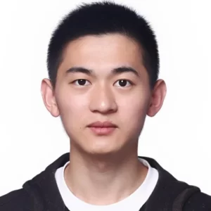
An Uncooled Short-wave Infrared GaAs Imager
Indium gallium arsenide (InGaAs) cameras are the state-of-art technology for short-wave infrared (SWIR) (950-1700 nm) imaging, which is highly demanded in military and defense, industry, and civilian where silicon (Si) detectors are no longer sensitive. However, the production of InGaAs sensors involves high-cost epitaxial growth, commonly Metal-Organic Chemical Vapor Deposition (MOCVD), and complex device fabrication processes. We report here, for the first time, an uncooled short-wave infrared imager based on a semi-insulating GaAs substrate, free of epitaxial growth. By simply depositing Au and ITO as top and bottom contact on semi-insulating GaAs wafers, an obvious sub-bandgap photoresponse is observed (Figure1b). In this talk, we will introduce its performance, clarify how the native defects contribute to SWIR photodetection at room temperature, show wafer-scale detector uniformity, and demonstrate single-pixel imaging. Further strategies for enhancing the detector performance will also be discussed.
Mr. Bian is a second-year Ph.D. student under the supervision of Prof. Lan Fu of the Australian National University. In the past 6 years, he focused on solar-driven photothermal processes for clean water production at Nanjing University (China). He proposed and fabricated a new design of a TiN-based solar-vapor generator used carbonized bamboos and magnolia for excellent solar vapor generation (>3L m-2 h-1 under 1-sun, enough for the daily needs of adults), developed an energy down-conversion strategy for clean water generation and solute recovery which were featured by ACS Axial, Advanced Science News, and SmartWaterMagazine.

JP Ndabakuranye
Bilirubin sensing – lessons learned and future perspectives.
Micromolar bilirubin (BR) levels (10 – 600 µ) historically have been primarily linked to the severity of neonatal jaundice and cirrhosis. Given their morbidity and mortality outcomes, continuous monitoring in the first week of birth for jaundice and in the long term for cirrhosis is paramount. The current clinical BR assessment standard is carried out in pathology laboratories involving invasive blood drawing and suitability for point-of-care (PoC) applications is limited due to complexity, high cost, and volumetric sizes. Specifically in paediatrics, drawing blood is a specialised job, and the measurement necessitates an invasively obtained large blood volume, causing anxiety to the mother and trauma to the infant. These approaches are thus not well-suited for the current global shift toward PoC and IoT-based wearable diagnostics.
On the other hand, despite significant progress in BR detection at the micromolar level, reliable detection in the nanomolar range remains a challenge. Achieving high sensitivity, specificity and accuracy at these ultralow levels is crucial, as recent evidence strongly links BR to chronic heart, lung, and neurological disorders. Accurate detection is also essential for developing diagnostic protocols to effectively monitor BR levels at nanomolar ranges for the aforementioned blind spots.
Herein, we review the latest BR assessment techniques in the micromolar range, emphasising current challenges and future opportunities in pediatric health and hepatic screening. We explore photonic techniques that could enable precise BR measurement at nano/picomolar ranges, including fluorescent quantum dots, guided-mode resonance, plasmonic cavity sensing, etc. This presentation may be valuable for clinicians, researchers, engineers, and policymakers.
Dr. Jean Pierre Ndabakuranye earned his PhD in Optoelectronics and Biomedical Engineering from the University of Melbourne in 2023. He is currently a research fellow at RMIT University, where his work focuses on biomedical optics, biosensing, and microelectronics. His primary area of interest is miniaturised point-of-care (PoC) diagnostics, particularly the development of portable, wearable, and implantable sensors.

Ivan Zhigulin
Narrowband Electroluminescence from Colour Centres in Hexagonal Boron Nitride
Wide bandgap materials such as hexagonal boron nitride (hBN) host color centers that act as quantum light emitters that are optically pumped and display narrowband emission suitable for quantum technologies. However, for on-chip and scalable quantum photonic circuitry, electrical excitation is highly sought after. By leveraging the van der Waals nature of 2D materials we are able to design heterostructures that build on quantum properties of charge carriers, such as tunneling, to realise electrical excitation of colour centres that emit narrowband light within the range of ultraviolet to near infrared. This work discovers novel key achievements in the field; a new method of activating isolated colour centres in hBN, electrically driven excitation that doesn’t utilise a p-n junction device, and mechanisms behind colour centres operation at cryogenic and room temperatures. Activated emitters demonstrated minimal temporal fluctuations over time in zero phonon line parameters, maintaining centre wavelength fluctuations below 1 nm and linewidth values around 0.5 nm. The electrically driven colour centres displayed linearly polarized emission, indicative of single optical transition. Additionally, electrically driven transitions were stable at cryogenic and room temperatures, where the room temperature spectral compositions mirrored typical hBN quantum emitters excited optically. The localised and non-classical nature of emissions was confirmed via second order autocorrelation measurements.
Ivan Zhigulin completed his Bachelor of Science major in Nanoscience & Technologies degree at the University of Sydney in 2020, and is currently at the final stage of his PhD candidature at University of Technology Sydney where he studies single photon emitters. Driven by the unique properties of 2D systems and specifically hBN, Ivan’s primary research focus is on the fabrication and characterisation of optoelectronic quantum devices from hexagonal boron nitride (hBN). Utilising Stark effect in various device geometries, he was able to further characterise hBN quantum emitters. Recently, Ivan’s proficiency in 2D heterostructure engineering led to successfully tackling a longstanding problem – electroluminescence (EL) from visible colour centres in hBN, a significant milestone in the field.

Xiaoying Huang
High-quality single photon sources from bottom-up single quantum dots in InP micro-ring resonators
The key elements for quantum photonic circuits are on-demand nonclassical light sources, a versatile photonic logic, the ability to store quantum information, and highly efficient detectors, directly integrated on-chip [1] . Ring resonators play an important role in the success of quantum photonics, because the ability to integrate with quantum dots and optical waveguides. [2] However, the current biggest obstacles for on-chip solid-state quantum emitters is the realization of deterministically fabrication of single quantum dots in optical cavities. [3] we have successfully combined the droplet epitaxy with selective area epitaxy of MOCVD to achieve scalable and deterministically growth of single quantum dots in nanowires in our previous work. [4] Here, we further extend this technic and successfully couple the single emissions into whispering gallery mode of InP micro-rings with different diameters. Our study paves the way for the development of future on-chip scalable quantum photonic networks for quantum information technologies.
Xiaoying Huang is a PhD student at the TMOS Centre Australian National University under supervision of Prof Hoe Tan. Her research project is focusing on selective area epitaxy in MOCVD system to achieve bottom-up single quantum dot in various optical cavities directly for the single / entangle photon sources applications.

Tongmiao Fan
Quantum Photon Pair Generation from Nonlinear Metasurfaces
Quantum technologies are garnering global attention for their transformative potential in society. Central to these advancements are quantum photon pairs, which are pivotal in quantum imaging, communication, and computing. The spontaneous parametric down conversion (SPDC) process, facilitated by second-order susceptibility in materials, is a key method for generating quantum-entangled photon pairs. While nonlinear crystals have been extensively researched for SPDC, nonlinear metasurfaces offer distinct advantages such as the ability to generate custom quantum states, ease of integration, and scalability.
Our team proposes and demonstrates a novel mechanism for producing optically tunable quantum entanglement using a nonlinear semiconductor metasurface. Leveraging the symmetry breaking of nonlinear current, we experimentally reveal a new mechanism for generating optically tunable biphoton entanglement from a semiconductor metasurface incorporating ⟨110⟩ InGaP nanostructures. We are exploring a potential collaborative project aimed at achieving and utilising hyper-entanglement from the InGaP metasurface.
In another project, we experimentally showcased the engineering of the biphoton spectrum from a nonlocal metasurface by manipulating a pump beam’s spatial shape. This approach allows for the creation of arbitrary biphoton spectrum by shaping the pump beam in k-space, potentially leading to on-demand spectral entanglement generation with nonlinear metasurfaces for quantum information processing applications.
Furthermore, we present the first demonstration of an enhanced SPDC process using a 2D material metasurface constructed from 3R-MoS2 [3]. The nano-resonators within this metasurface support quasi-bound states in the continuum (qBIC) with an exceptionally high quality factor of up to 381, resulting in a 20-fold increase in SPDC rate. This breakthrough opens new avenues for utilizing triple-resonance van der Waals material metasurfaces in quantum photon pair generation.
Mr Tongmiao Fan completed his master’s degree in Quantum Technology at the Australian National University, where he focused on the fields of metasurfaces and photon-pair generation. He is currently pursuing a PhD under the esteemed guidance of Professor Andrey Sukhorukov.
Day 3 – Thursday 21st November 2024

Mark Brongersma
Meta-Imaging of Texture and Tissue
Metamaterials are a new, emerging class of high-performance materials that derive their unique, physical properties from the way they are structured. In the first part of this presentation, I will focus on the creation of 2-dimensional metamaterials (i.e. metasurfaces) by nanopatterning thin layers of semiconductors and metals. I will argue that metasurfaces are ideal building blocks for next generation sensing and imaging technologies. For example, I will show how one can create transparent optical sensors on glass substrates that can extract valuable information from an optical scene. I will also discuss the use of integrated metasurfaces can enable new imaging modalities, such as the imaging of texture.
In the second part of my talk I will explain how metamaterials concepts can be used reduce the opacity of tissue and skin due to unwanted light scattering from the refractive index mismatch among its components. Conventionally, water and/or liquids need to be removed to make biological tissues transparent by minimizing refractive index mismatch; however, this process hinders achieving transparency in live tissues. I will discuss the counterintuitive observation that strongly absorbing molecules can achieve optical transparency in live biological tissues. I will highlight the physics behind this phenomenon and show that when strongly absorbing molecules dissolve in water to form a liquid metamaterial, they can modify its refractive index via the Kramers-Kronig relations to match that of high-index tissue components like lipids. We demonstrate that this straightforward approach can reversibly render the mouse abdominal wall transparent to allow visualization of the digestive tract peristalsis and image myenteric ganglia microscopically.
Mark Brongersma is the Stephen Harris Professor of Engineering at Stanford University. He leads a research team of ten students and five postdocs. Their research is directed towards the development and physical analysis of new materials and structures that find use in nanoscale electronic and photonic devices. He is on the list of Global Highly Cited Researchers (Clarivate Analytics). He received a National Science Foundation Career Award, the Walter J. Gores Award for Excellence in Teaching, the International Raymond and Beverly Sackler Prize in the Physical Sciences (Physics) for his work on plasmonics, and is a Fellow of the OSA, the SPIE, and the APS. Dr. Brongersma received his PhD from the FOM Institute AMOLF in Amsterdam, The Netherlands, in 1998. From 1998-2001 he was a postdoctoral research fellow at the California Institute of Technology
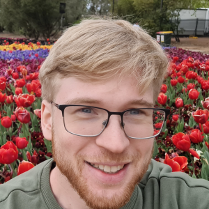
Lukas Jaeger
Optical coupling of lasing InP nanowires
Semiconductor nanowires are a keystone in the miniaturization of optoelectronic devices, because they bring the potential to realize compact nanolasers. This is due to their waveguiding properties, high optical gain and low power consumption. For many nanoscale photonic applications, the evanescent coupling between two adjacent nanowires yields interesting consequences, such as mode-splitting and changes to the farfield emission. In recent years the optical resonances in nanowire pairs have been investigated for Si, GaN and CdS nanowires for various arrangements and with disparate measurement techniques. Here we grew InP nanowires using MOCVD with precise arrangements: in pairs and triplets with a defined gap. Micro-photoluminescence and back-focal-plane measurements with a pulsed 532nm laser were conducted and compared with FDTD simulation results.

Laura Daniela Valencia Molina
Nonlinear Optical Response of Gold Nanoparticles Interacting with MoS2 Monolayers
Transition metal dichalcogenides (TMDCs) have interesting optical properties when thinned down to the monolayer (ML) state, including broken inversion symmetry and direct band gap, making ML-TMDCs interesting materials for nonlinear optics. Importantly the structure of the χ2 tensor of 2D TMDCs imposes a sign flip for the SHG for a circularly polarized fundamental harmonic field. Recent studies have shown that combining ML-TMDCs with plasmonic nanoantennas may control the SHG polarization and significantly increase the SHG signal. In this study, gold nanoparticles (AuNPs) were deposited on top of SiOx (5nm), ML-MoS2, and fused silica substrates (see Fig 1B).
Here, we investigated the second harmonic generation (SHG) response of ML-MoS2 interacting with AuNPs under NIR circular polarised light by analyzing its polarisation nonlinear response with the Stokes parameters. The results show that in contrast to similar experiments performed for circularly polarised PL from valley-polarised exciton populations in such systems [4], the presence of AuNPs preserves the circular polarisation of the incident light, , leading a depolarisation of the SHG response of the AuNP/ML-MoS2, while for the ML-MoS2, the two fundamental frequency photons of a given helicity are converted into one photon of opposite helicity as shown in Fig. 1 C and D. Understanding and controlling the SHG can, therefore, be essential for tailoring polarisation of light, which is important for practical applications using optical nonlinearities such as all-optical devices, frequency combs, high-order harmonic generation and multiphoton microscopy.
Laura was Born in Colombia. She completed her Bachelor’s degree in Physics at the University of Quindio in Colombia before pursuing a Master’s degree in Sciences at Center of research in Optics (CIO) in Mexico. During her time at CIO, she conducted research on 2D materials and shape memory polymers for potential biomimetic applications. Currently, Laura is engaged in a dual PhD program with the Australian National University and Friedrich Schiller Universität Jena. Her research is centered around metasurfaces for infrared-to-visible imaging, exploring novel designs that can enhance the capabilities for imaging systems. Laura is looking for making strides in this area of research, aiming to advance imaging technology and its applications. Her research interests are metamaterials, photonics, 2D materials and Imaging.
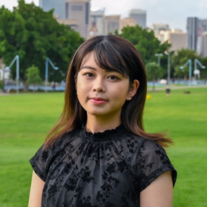
Karin Yamamura
Quantum Efficiency of blue colour center in hexagonal boron nitride
Color center in hexagonal boron nitride (hBN) have emerged as promising candidates for single-photon emission, a key component in quantum photonics [1]. The ability to precisely position B-center using electron beam irradiation and achieve highly reproducible emission wavelengths makes them highly attractive for practical applications [2,3]. In this study, we focus on measuring the quantum efficiency (QE) of single B-centres engineered within a 35 nm thick hBN flake using electron beam irradiation. By strategically altering the local dielectric environment with an additional 250 nm hBN layer, we observed significant changes in the photoluminescence lifetimes of the emitters. These changes enabled us to accurately determine the QE of B-centres in thin hBN flakes, revealing values exceeding 40%. Furthermore, we explore two distinct methods for quantifying the QE of B-centres in thicker hBN flakes, suggesting that near-unity QE is attainable with appropriate Purcell enhancement. Our findings underscore the potential of B-centres in hBN for developing efficient single-photon sources, paving the way for advanced quantum technologies.
Karin is a PhD candidate at UTS under the supervision of Prof. Igor Aharanovich and Prof. Milos Toth. She completed her Bachelor of Science in Nanotechnology (Honours) at UTS in 2021. Her research is focused on the characterization of materials for applications of single photon emitter in telecommunication region, and the creation and modification of quantum emitters using charged particle microscopy techniques.

Gia Parish
Defence research and innovation ecosystem in Australia – a work in progress.
The landscape for undertaking defence research in Australia has been changing rapidly with the government, through Defence Australia, setting new priorities and overhauling funding mechanisms and streams, and relationship management. At the same time, AUKUS offers new opportunities for conducting defence research across borders and particularly with the US and UK. But there are challenges both in scale and scope of funding, as well as the underlying culture [1]. This talk will provide some insights into the current state of the defence R&I ecosystem in Australia, and explore what Defence, government, industry, academia are doing or need to change individually and together to better advance our national (and international) defence & security endeavour.
Giacinta (Gia) Parish is Director, Defence & Security Institute and Professor, School of Engineering at the University of Western Australia; and a Director on the Board of AROSE. Professor Parish joined UWA after completing a PhD at the University of California, Santa Barbara as a Fulbright Scholar. She has a multidisciplinary background in electronic engineering, materials science and chemistry; particularly advanced semiconductor materials and device technologies. Her current research focus is chemical, bio- and infrared sensors for environmental and industrial monitoring and defence applications. Professor Parish has co-authored around 150 international publications, with close to 3000 citations, and was an inaugural Women in Technology WA ‘20 in 20’ award winner in 2018.

Mario Hentschel
Fabrication in Nanophotonics: Techniques and Applications
Manipulating light on the nanoscale has become a central challenge in metadevices, resonant surfaces, nanoscale optical sensors and many more, requiring precise control over shape, composition, and arrangement of nanoscale optical systems. Nano- and microfabrication has thus become a central and enabling tool in this research. While commercial nanofabrication established major fabrication strategies along well-defined lines, in research the boundary conditions change frequently, which requires to adapt establish processes to new materials and material classes. In this talk I will give insight into some of our recent work in Mie-tronic and plasmonic systems with special consideration of nanofabrication techniques, touching on Mie voids for loss-free nanoscale light confinement in air, chiral plasmonics, electrically switchable active plasmonic systems based on metallic polymers, and other nanofabrication techniques.
Dr. Mario Hentschel is a physicist at the University of Stuttgart’s 4th Physics Institute, where he leads the cleanroom and nanostructuring facilities. His work focuses on nanophotonics, plasmonics, and advanced techniques in light manipulation at the nanoscale. Among his recent accomplishments, Dr. Hentschel has gained significant attention for creating the world’s smallest version of Wassily Kandinsky’s “Improvisation 9,” a feat achieved through ion beam lithography. This technique enabled him to replicate the painting on a silicon wafer at an ultra-high resolution of 36,000 dpi, fitting the artwork into an area smaller than a human hair. This innovative work has implications for both art preservation and applications in sensor technology and nanophotonics.
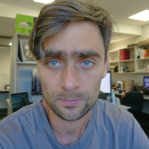
Oleg Banik
Tunable MEMS metasurface for thermal infrared filtering
The formation of terahertz beams with inhomogeneous polarization states and phase singularities attracts growing attention due to potential applications of such beams in telecommunication, material characterization, and imaging. Although there exist many approaches to generate vortex beams in the terahertz frequency range including spiral phase plates, beam shaping metasurfaces, forked gratings, liquid crystals, a recently emerged method involves the transformation of a circularly polarized beam through its interaction with a metasurface supporting bound states in the continuum (BICs), and it still remains unexplored. In this work, we study a vortex beam generator based on a two-dimensional metasurface membrane supporting the bound state in the continuum. Unlike typical structures forming beam with the optical angular momentum (OAM) through phase modulation in real space, the metasurface membrane has winding topologies of resonances around the BIC in the momentum space. This enables a helicoidal Pancharatnam-Berry phase and spin–orbital interaction in the real space beam. We study this effect by calculating the band structures and quality factors of metasurfaces with different symmetries and analyze BICs near the Γ point of the momentum space. We characterize the polarization states and show that they have winding configuration in the far field. We prove the formation of vortex beams with OAM of 1 and 2 in the terahertz range via modelling circularly polarized Gaussian beams incident on the metasurfaces.

Benjamin Russell
Thermal Tuning mechanisms for Switchable Spectral Filters and Their Applications
This abstract includes a collaboration with the RMIT TMOS node that has been underway since mid-2024. It has received input from Krishna Murali, Peter Elango, Phuong Le Yen, and Ying Zhi Cheong. We exploit two refractive index tuning mechanisms to modulate the infrared spectral properties of two different periodic subwavelength metasurfaces. The volatile, thermo-optic effect in silicon, and the stable, amorphous-to-crystalline phase change in antimony triselenide (Sb2Se3) are considered in a tunable narrow bandpass filter, and a broadband switchable binary filter respectively. We have experimentally measured a 138 nm redshift of an isolated spectral resonance in a 2D silicon zerocontrast grating (ZCG) that was initially optimized to possess a 29 nm wide bandpass feature at 3438 nm. This was achieved by sweeping the sample temperature from 93 K to 873 K. Additionally, we have optimized the dimensions of a 2-D photonic crystal consisting of square holes in a 120 nm thick Sb2Se3 film on a quartz substrate. We optimize the hole period and width to maximize transmission in the Sb2Se3 film’s crystalline phase and maximize reflectance in the film’s amorphous phase. This will enable the creation of static, ultrathin, reprogrammable amplitude masks with an arbitrary spatial profile via selective amorphization of the metasurface using an appropriate laser writing tool, for example, creating a bespoke Fresnel zone-plate (Fig. 1f). The surface can in theory be erased through thermal annealing as in
Melbourne born but Warrnambool raised, Ben has had his mind set on physics ever since the BBC documentary ‘Absolute Zero’ premiered 2008. In 2015 he returned to Melbourne to complete a Bachelor of Science and a Diploma of Music in Trombone Performance at the University of Melbourne. Finding optics to be the discipline he was most interested in, he remained at the University to undertake a Master of Science in Physics under the supervision of Professor Ken Crozier, which was completed in 2020. Ben joined TMOS in 2021 with the commencement of his PhD in physics, hoping to build on the research groundwork laid down during his master’s degree. He wishes to remain in optics and photonics for the foreseeable future, taking a particular interest in the development of dielectric metasurfaces and their incorporation in microspectrometer systems. His work also relies on algorithmic approaches to spectroscopy, chemical classification, and metasurface design.
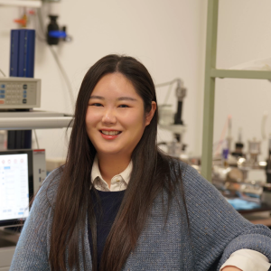
Yan Liu
MEMS-based Tunable Optical Filter with Broad Bandwidth
Tunable Microelectromechanical System MEMS optical filters using integrated micromirrors are well known in infrared sensing technologies. The transmission wavelength of a MEMS Fabry Perot spectrometer is controlled by electrostatic actuation of movable mirrors. The stability of this actuation mechanism relies on the balance between the electrostatic actuation force and the mechanical restoring force provided by the membrane support structure. An electrostatic force is generated between two parallel conductive plates electrodes that causes movement of the MEMS. However, the actuation range of MEMS devices is constrained by the snap down pull in effect, where a runaway electrostatic force eventually overcomes the restoring forces as the moving mirror approaches the fixed one.
This paper presents a novel approach to extend the actuation range of tunable optical filters based on the concept of floating electrode electrostatic actuator consisting of two series connected MEMS capacitors. In this design, only a portion of the membrane structure is movable while a solid post fixed size supports membrane and helps tune the capacitance ratio between the two capacitors. Dynamic adjustment of this ratio can allow the device to extend the snap down beyond the traditional limit of one third gap. In applying this extended travel range approach to tunable optical filters, the central optical area of the membrane is actuated by four series connected floating electrodes. This very promising design extends the gap distance between the top and bottom electrodes by approximately 60.7 percent providing a broadband tunable range of the spectrometer from 1.2 um to 1.75 um.
Yan Liu is a PhD candidate in the School of Engineering at the University of Western Australia under the supervision of Professor Lorenzo Faraone and Professor Dilusha Silva. She is pursuing a doctoral degree in the Microelectromechanical systems MEMS research area. Her current research is about large area MEMS structures for tunable optical filters, which has shown immense promise for developing infrared sensing applications over the past decades.
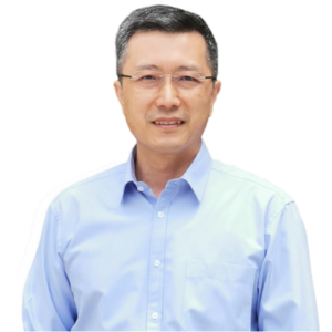
Jinghua Teng
Van der Waals and Phase Change Materials for Tunable Flat Optics
Tunable flat optics by employing active optical materials responding to external stimuli can enhance the capability and adaptability of an optical system. Chalcogenide alloys have phase changes between amorphous and crystalline with temperature changing across the phase transition temperature, which induce both refractive index and electrical conductivity changes and have been applied to diverse tunable micro-nano-optical devices across wide spectral range. The unique properties of 2D materials such as the strong quantum confinement, bandgap tuning and flexible integration with different substrates bring many new opportunities to photonics and tunable metaoptics. In this talk, I will give a brief review of tunable and reconfigurable metaoptics followed by introducing some of our recent works using chalcogenide phase change materials for tunable Tamm plasmonic response for biosensing, color coding, wide angle perfect absorption and light beam switching, as well as van der Waals materials for electrically tuning of refractive index and phase through excitonic effect, and flat lens focusing through linear electro-optic effect.
Dr Jinghua Teng is a Principal Scientist at the Institute of Materials Research and Engineering IMRE under Singapore’s Agency for Science Technology and Research ASTAR and an Adjunct Professor at Nanyang Technological University. He received his PhD in Optoelectronics from the National University of Singapore and has a strong background in academic research and industry driven technology development. His extensive work in nano optics, metamaterials and THz technology has earned him numerous publications with over 230 journal papers, five edited or authored books or chapters and 29 primary patents.
Shuo Ma
Damage free lift off of HgCdTe thin films for future curved IR detector applications
Curved infrared IR detectors offer a range of benefits that traditional flat IR detectors cannot provide such as enhanced field of view, improved imaging performance, and reduced SWaP size, weight, and power for IR imaging systems. To achieve HgCdTe curved IR detectors, it is essential to obtain free standing HgCdTe thin films which can be transferred to other substrates for curved detector fabrication. This study aims to study the epitaxial lift off of HgCdTe thin films by using a unique MgTe sacrificial layer and demonstrate the feasibility of this technology for making high performance IR detectors. HgCdTe thin films were grown on CdZnTe substrates with a MgTe sacrificial layer in between using Molecular Beam Epitaxy. They were then lifted off from CdZnTe substrates and transferred to Si substrates for further material characterization. Mid wave infrared photoconductors were also fabricated and characterized by using the HgCdTe thin films before and after the epitaxial lift off. Comprehensive characterizations suggest that the epitaxial lift off process is damage free. Photoconductors fabricated with the lift offed HgCdTe thin films present excellent device performance peak responsivity of 495 V/W and detectivity of 1.5×10¹⁰ Jones at 77 K and imaging quality comparable to those before the lift off.
Shuo received his bachelor degree in engineering from Southwest University in 2018 and master degree in professional engineering from EECE of the University of Western Australia in 2020. After graduation, he decided to pursue the doctoral degree in UWA. He is currently a PhD student in Microelectronic Research Group MRG. His research interests include HgCdTe material growth, material characterization, device fabrication and testing for curved thin film infrared detectors applications.
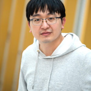
Mingjie Yang
Optical Glucose Sensor Using 1600 1700 nm Near Infrared NIR Light
Blood glucose is crucial for diabetes diagnoses and treatments, but invasive sampling methods have drawbacks. Non invasive NIR spectroscopy based optical glucose sensing has gained attention but faces challenges due to the strong absorbance of NIR light by water and the need for complex equipment. Here, spectroscopic analysis has identified four distinct glucose fingerprints at specific NIR wavelengths 1605, 1706, 2145 and 2275 nm. Utilizing a surface mounted LED with a spectral range of 1600 1700 nm and focusing on the most prominent peaks at 1605 and 1706 nm, a miniaturized and non invasive glucose sensor was developed. The device successfully detects in vitro assays of glucose solutions within the physiological range of 50 400 mg/dL, attaining a limit of detection as low as 10 mg/dL. The findings demonstrate the feasibility of NIR spectroscopy based glucose sensing and its potential applications in non invasive point of care diagnostics, with the potential for extension to other biomarkers in future.
Mingjie Yang is a PhD candidate at RMIT University with an educational background in Engineering. After earning a Bachelor of Engineering Electrical and Electronic from Sichuan University China in 2012, he advanced his studies at Monash University Australia, where he received a Master of Engineering Materials in 2019. His academic journey led him to hold positions as a Research Assistant at both Monash University and RMIT University, where he honed his expertise in Nanofabrication, Electronics Development, Immunosensor Fabrication, and NIR Spectroscopy.
Ingrid Ward
Fingerprinting the Past FTIR as a method for tracing human activity in the Australian cultural landscape
Archaeology can be likened to a detective story where investigators examine the remnants of human activity thousands of years after the fact. The scientific methods used to analyse ancient organic and inorganic materials closely resemble those used in modern forensic laboratories, particularly micro analytical techniques. This presentation presents case studies from Australia that demonstrate the use of Fourier Transform Infrared Microspectroscopy FTIRM and associated microarchaeological methods in uncovering trace evidence linking artifacts to past human activities.
Fourier transform infrared FTIR spectroscopy and Raman spectroscopy are powerful analytical techniques that generate a vibrational fingerprint of a broad range of materials. In Australia, however, more attention has been given to durable components of the archaeological record, such as stone tools, using traditional analytical techniques. This has led to a gap in the application of vibrational spectroscopic methods to inorganic and more especially organic elements, including bone, shell, wood, pigments, plant resins, fibers and so on, where the greatest potential for FTIR spectroscopy resides.
The case studies presented include the use of synchrotron based FTIRM SR FTIRM at the Australian Synchrotron ANSTO for chemical analysis of minute archaeological samples at the micron scale. The first case explores residues found on small stone tools excavated from Pleistocene cave deposits, possibly associated with early hafting technologies. A second study applied SR FTIRM to analyse micro morphological thin sections of bone fragments from Pleistocene archaeological sites in NW Australia.
What emerges from these studies is the need for regional and nationally relevant reference libraries, particularly given Australia’s unique flora and fauna. Future developments and archaeological applications in FTIRM are also discussed. While we may never fully reconstruct the past, a forensic approach enables archaeologists to provide well founded expert opinions that stand up to scrutiny. In this presentation, I’ll leave the final judgment to you.
Dr Ingrid is a renowned geoarchaeologist known for her multidisciplinary approach to investigating both terrestrial and marine archaeological landscapes. She has authored key papers advocating for a geoarchaeological perspective on submerged landscapes across Europe and northwest Australia, with a focus on sedimentary landscapes and the environmental context that preserves archaeological remains. Her research provides insights into human landscape dynamics at both macro and micro levels.
Day 4 – Friday 22nd November 2024
Haoran Ren
Synthetic metasurfaces for advanced photonic functions
Ultrathin metasurfaces composed of a planar array of subwavelength structures offer a versatile platform in broad photonic applications. They can shape the wavefront of light across multiple degrees of freedom, including amplitude, phase, polarization, wavelength, and orbital angular momentum. However, single task metasurfaces designed with single type meta atoms the unit cells of a metasurface device suffer from limited photonic functions, such as restricted bandwidth for metalenses and limited polarization sensitivity.
To enhance metasurface functionalities without increasing the aperture size, synthetic multifunctional metasurfaces have recently been explored. Spectral domain synthesis of phase functions implemented by metasurfaces enables precise pulse shaping and the generation of spatiotemporal beams, allowing the structuring of ultrafast beam pulses with complex wavefronts in an ultrafast time domain. Multifunctional interleaved geometric phase metasurfaces have been employed to achieve multiple phase functions. However, their use of single type meta atoms results in significant crosstalk. Additionally, synthetic apertures based on the segmentation mixture of multi task meta atoms have been developed to achieve multiple polarization detection. In this case, a light beam must scan across all the segmented sections to perform different polarization measurements.
In this talk, I will present the design and fabrication of synthetic Fourier metasurfaces by multiplexing different photonic functions in the Fourier domain of the metasurface. Our generalized design and optimization of synthetic metasurfaces based on multi task meta atoms enable us to achieve large scale achromatic metalenses, as well as polarimetric imaging of arbitrarily structured light simultaneously. We believe our synthetic Fourier metasurfaces, harnessing multiplexed photonic functionalities, will find important applications in wavefront engineering, optical and quantum imaging, holographic displays, and spatiotemporal beam control.
Dr Haoran Ren is a DECRA Fellow leading the Structured Nanophotonics Group at Monash University, where he focuses on exploring light matter interactions at the nanoscale. His research, which draws from his fascination with optical physics, has significant applications across various fields in optics. Over the past five years, he has secured over 2 million in research funding, supporting his innovative projects and contributions.

Patrick Rufangura
Mid infrared enhanced thermal emission with germanium coupled silicon carbide surface phonon polariton on silicon
Thermal emitters have broad applications in gas sensing, thermal imaging, thermophotovoltaics, radiative cooling, and thermal camouflage. There is much interest in the mid infrared MIR thermal emitters, a spectral region where several gases, liquids, and solids exhibit vibrational absorption fingerprints. Natural emitters are bulky and exhibit a broadband, incoherent thermal emission, which hinders their use for various applications. Engineered nanostructures have proven to realize narrowband coherent thermal emission. Surface phonon polaritons SPhPs, which result from the coupling of electromagnetic EM field of incident photons and coherent oscillations of charged atomic species in polar materials, have recently attracted significant attention. The SPhPs can be supported in the MIR spectral region between longitudinal optical LO and transverse optical TO frequencies where polar materials exhibit a negative real part of permittivity. SiC is one of the polar materials that support SPhPs mode, and low intrinsic losses associated with the long scattering rates of the optical phonons in SiC allow the realization of sharp resonances with high Q factors. However, a significant momentum mismatch between free space photon and surface phonon inhibits their coupling into SPhPs. One way to launch SPhPs is to use the gratings coupler, which provides the missing light momentum.
In this work, we combine experiments with EM simulation based on Finite Element Method FEM to demonstrate SPhPs enabling absorption emittance enhancement in germanium gratings on SiC Si, which shows promise for MIR thermal emission. As anticipated, low emittance was confirmed from both simulations and measurements on bare SiC grating SiC Si due to the inefficient coupling of SPhP fields caused by the decay length of evanescent fields being larger than the thickness of SiC grating. On the other hand, a near unit emittance with a high Q factor of 190 was realized using a subwavelength 100 nm Ge grating on SiC, as confirmed by FEM simulation and experimental results. Here, Ge transparent to MIR radiations gratings reduce the decay length of the evanescent wave, enabling robust field confinement in the device and enhancing emittance.
Patrick Rufangura is a Postdoctoral Research Associate at the School of Electrical and Data Engineering, Faculty of Engineering and IT, University of Technology Sydney. His research focuses on electromagnetic simulations, nanofabrication, and IR characterization of graphene and silicon carbide based metasurfaces for mid infrared nanophotonics. He completed his BSc degree in Applied Physics from the University of Rwanda in 2011 and a master’s degree in sustainable environment and energy systems focusing on the design and characterization of wideband metamaterial absorbers for solar energy applications at the Middle East Technical University in 2015. He subsequently completed his PhD in Electrical and Data Engineering from the University of Technology Sydney in 2022, where he developed a model for a fundamental study of epitaxial graphene on silicon carbide on silicon for mid infrared nanophotonics. Currently, he is working on graphene SiC based narrowband thermal emitters and transmission filters for MIR applications.

Adrian Keating
The art of scientific presentation
This talk reviews the basics of how to deliver high quality, visually impressive presentations. The core focus is on avoiding ambiguity in the data and information being presented. Standard presentation styles will be considered, looking at pitfalls and approaches to avoid them. The discussion will cover common mistakes, including how fonts and colours can often confuse the audience. The talk is particularly well suited to students and ECRs working on developing their presentation styles and is hoped will encourage active discussions at the conference and within the various research groups.
Dr Adrian Keating is an Associate Professor in the School of Engineering at the University of Western Australia, focusing on micro electromechanical systems MEMS, microfluidics, and porous silicon. His research centres on the development of advanced micro sensing technologies, particularly in thermal and chemical sensing, which have applications in environmental monitoring and healthcare.
With over 160 publications, Dr Keating has made significant contributions to silicon micromachining and nanostructuring. His work bridges the gap between innovative engineering and practical applications, supporting advancements in biomedical devices and enhancing environmental monitoring solutions.