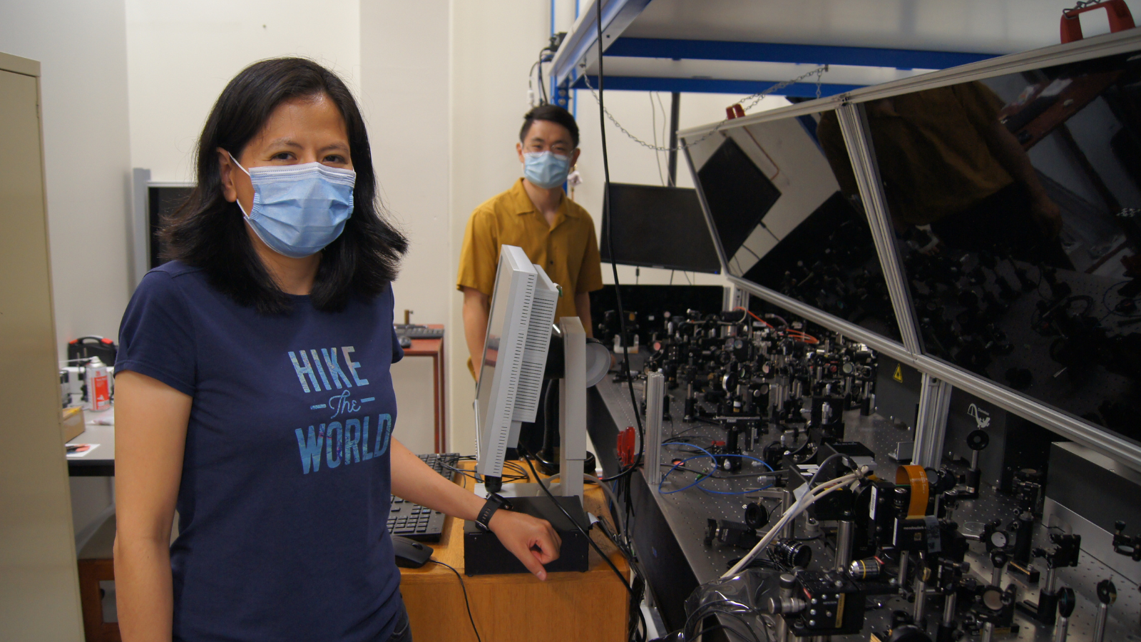
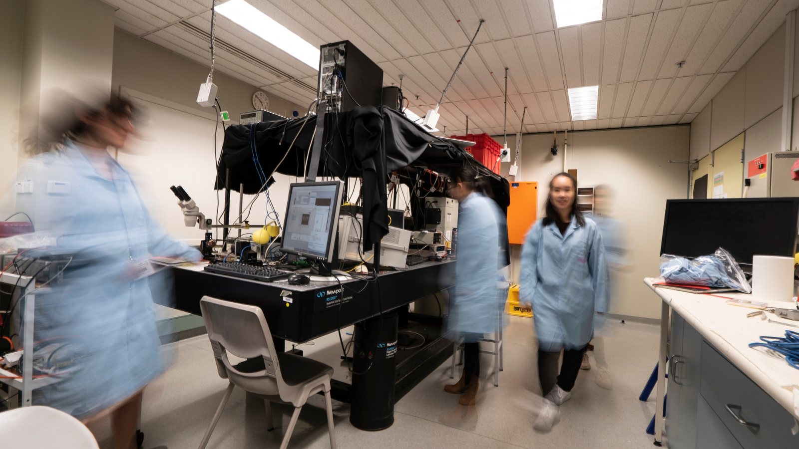
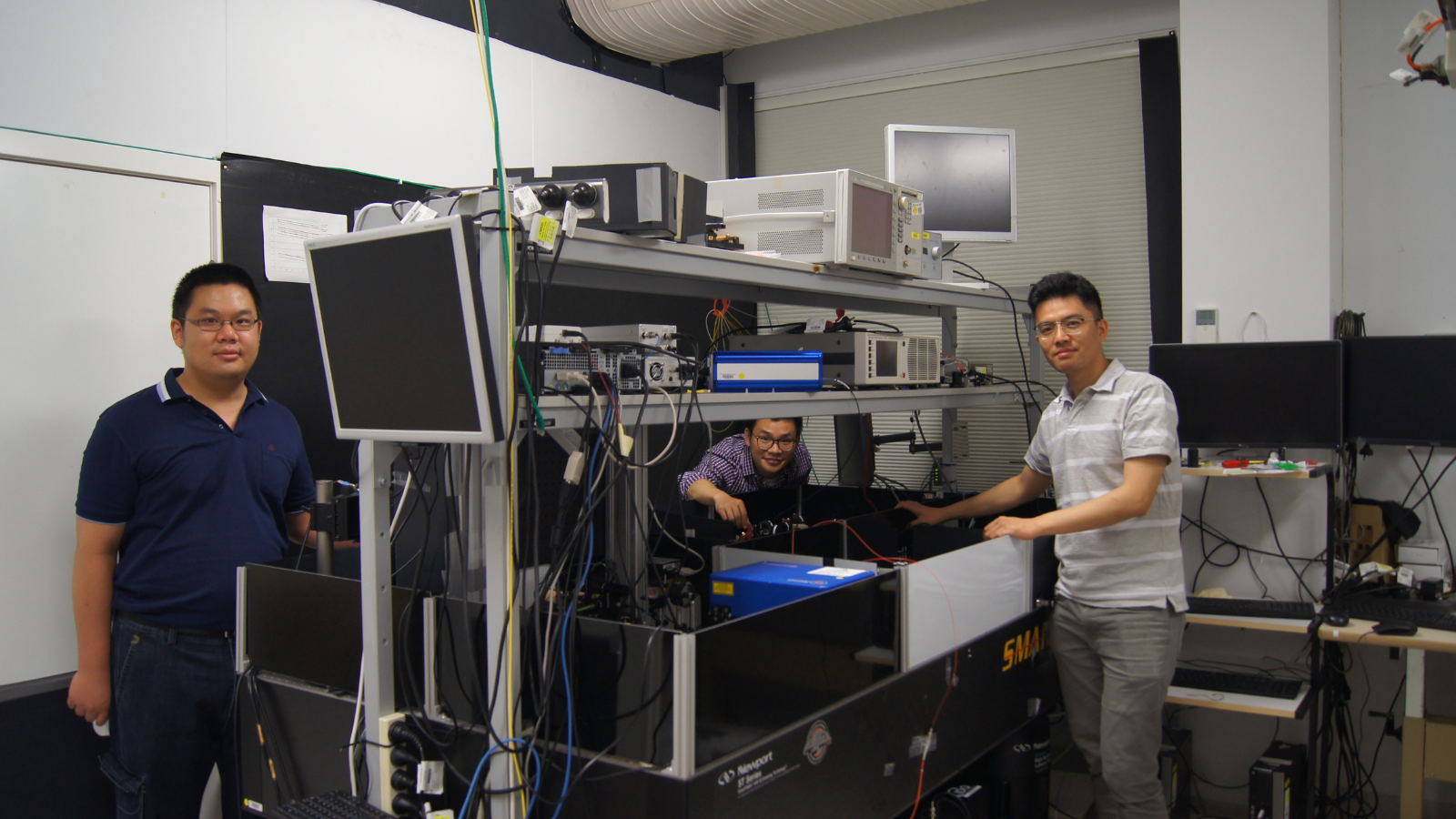
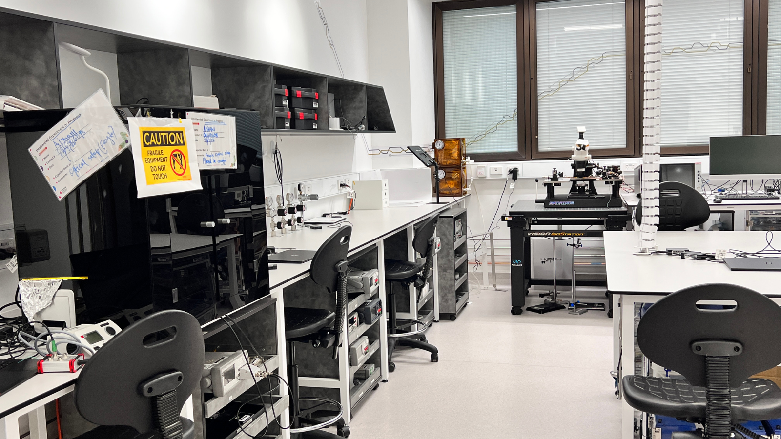
Australian National University
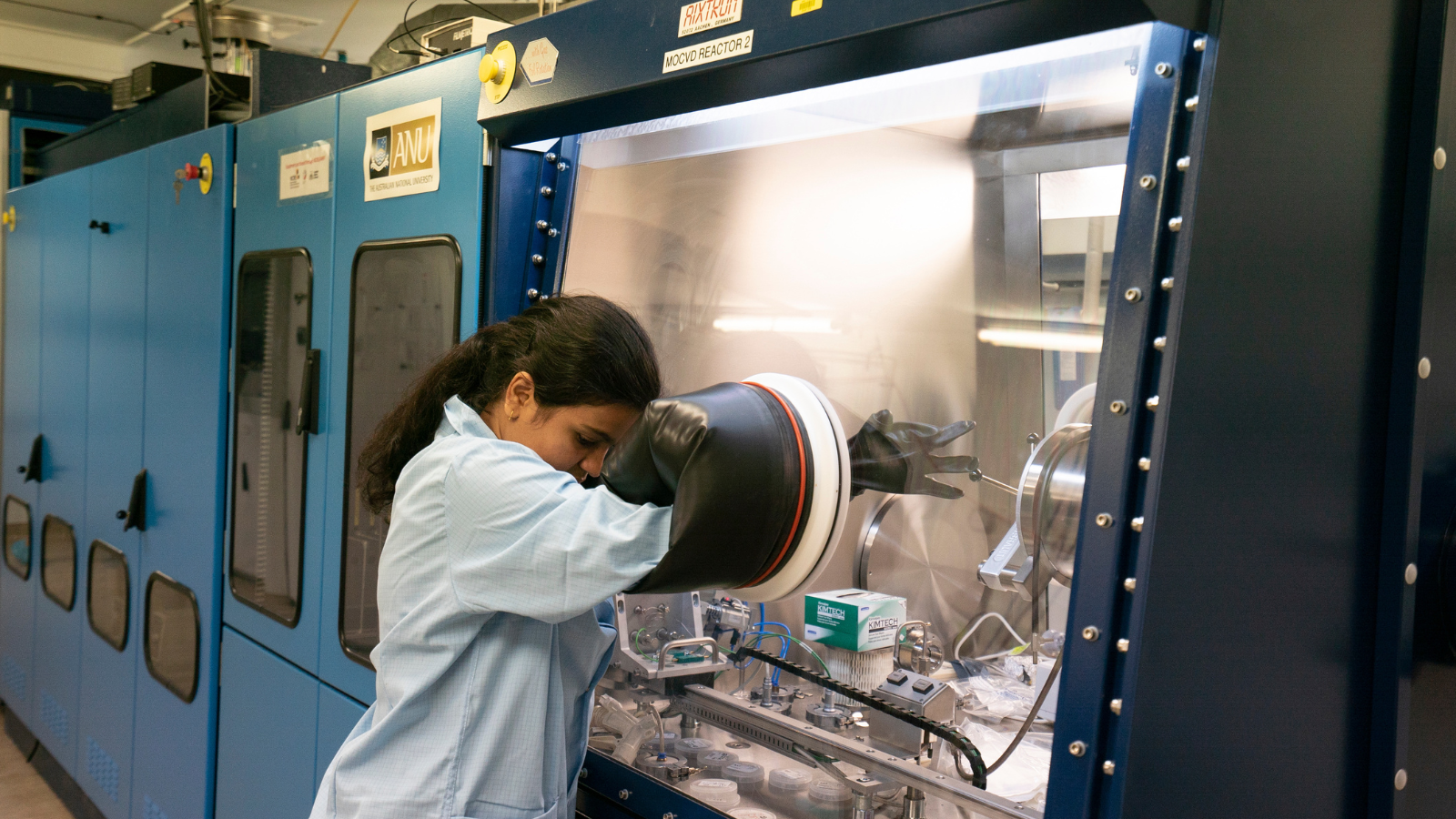
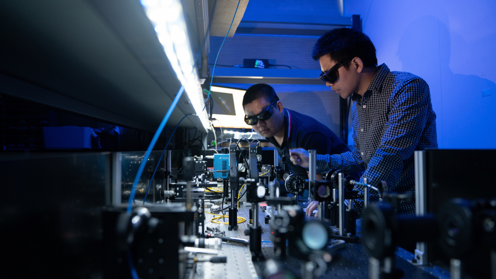
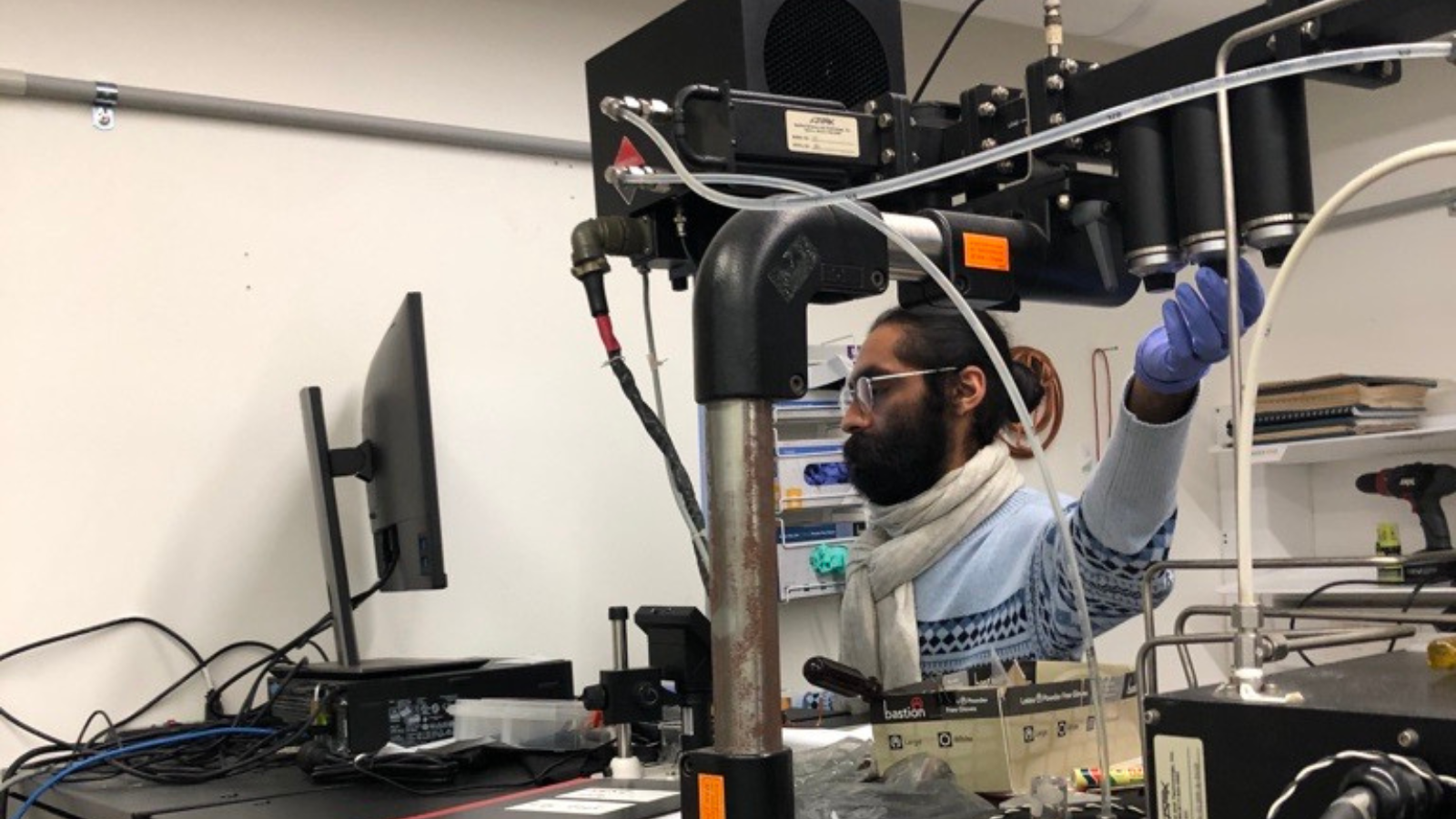
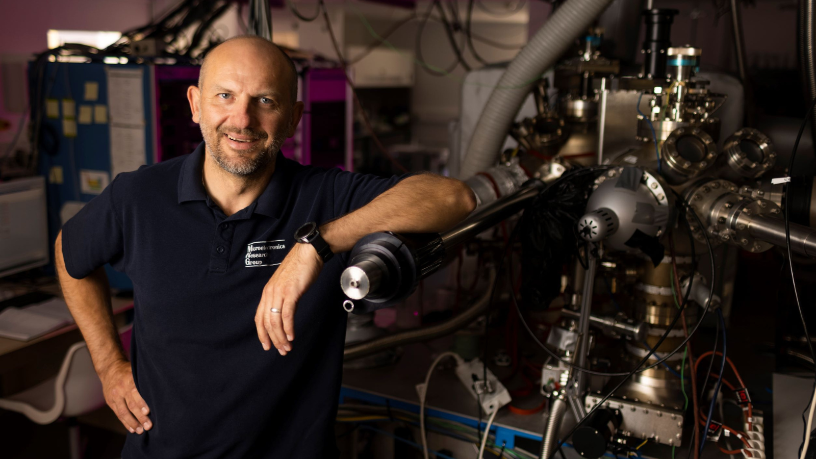
Through the Australian National Fabrication Facility, ACT Node, we operate an integrated III-V semiconductor facility for epitaxial growth, fabrication and characterisation of optoelectronic devices. Some of the flagship tools in the facility include:
- metal organic chemical vapour deposition systems for the growth of III-V semiconductors
- high-throughput, large area electron beam lithography system
- nanoimprint and optical lithography system
- focussed ion beam
- atomic layer deposition systems for metal oxides and nitrides
- plasma etching and deposition tools
- DC/RF magnetron sputtering system
- flip-chip and wire bonders
- cathodoluminescence and spectroscopic ellipsometer
RMIT
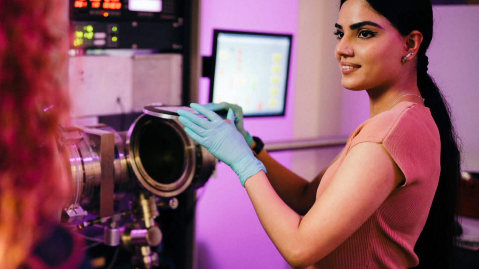
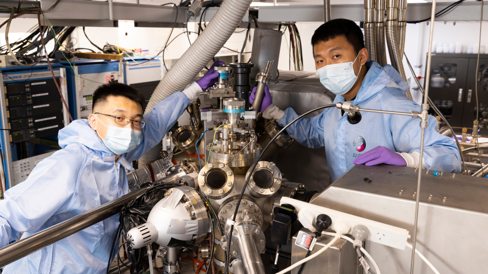
The Micro Nano Research Facility at RMIT is a $45 million, state-of-the-art cleanroom facility for materials synthesis, device fabrication, and device prototyping that is updated regularly to deliver new capabilities.
There are also specialised laboratories for micro/nanoelectronic device characterisation, flexible/stretchable electronics and integration, two-dimensional materials growth, nanoscale fabrication and 3D printing, and prototyping of wearable devices.
University of Melbourne
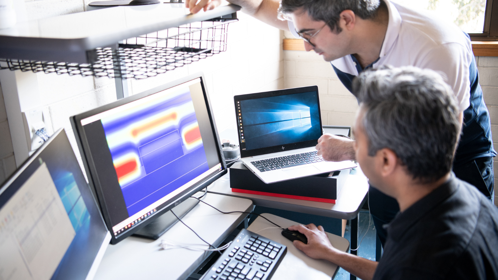
The University of Melbourne is a world leader in the physical sciences and engineering. CIs Roberts and Crozier are part of this vibrant intellectual environment, and have access to excellent experimental infrastructure. The University of Melbourne is a partner in the Victorian node of the Australian National Fabrication Facility headquartered at the Melbourne Centre for Nanofabrication (MCN), a state-of-the-art clean-room. The research groups of CIs Crozier and Roberts are active users of this facility. They also have excellent experimental and computing facilities available for at the University of Melbourne. Staff and students are members of the Optical Physics Group of the School of Physics and of Electronic and/or the Photonic Systems Group of the Department of Electrical and Electronic Engineering. They make use of the facilities within the Electronic and Photonic Systems Group and within other labs within the Optical Physics Group. This demonstrates the collaborative nature of the research environment for optics, photonics, and semiconductor devices at the University.
University of Technology Sydney
University of Western Australia
Acknowledgement of Country
The ARC Centre for Transformative Meta-Optical Systems (TMOS) acknowledges the Traditional Owners and their custodianship of the lands on which our teams operate. We pay our respects to their Ancestors and their descendants, who continue cultural and spiritual connections to Country. We recognise their valuable contributions to Australian and global society.