Quantum double-act the key to bright magnetic sensors
02 Dec, 2025
Physicists have solved the puzzle of glowing atoms in semiconductors that can be magnetically controlled.
The answer – that the emission actually comes from two coupled atoms – opens the way for researchers to design much more efficient quantum sensors, by leveraging the magnetic spin response of the emitter, said leader of the research group, Associate Professor Jean-Philippe Tetienne.
“This simple elegant model solved many puzzles in one strike. For researchers trying to explain their observations suddenly everything makes a lot more sense,” said A/Prof Tetienne, from the ARC Centre of Excellence for Transformative Meta-Optical Systems (TMOS) and the Royal Melbourne Institute of Technology (RMIT).

A sensitive and accurate quantum sensor for magnetic fields has potential for a wide range of uses, from material analysis to medical diagnoses.
The research, published in Nature Physics , was a joint effort between the University of Technology Sydney (UTS), led by Professor Igor Aharonovich (TMOS), and RMIT, led by Associate Professor Jean-Philippe Tetienne.
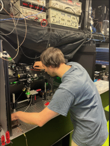
The team were investigating atomic emitters in the semiconductor hexagonal boron nitride (hBN). The emitters are irregularities in the semiconductor lattice – individual atoms that are out of place or missing – and when light shines on the semiconductor these atoms gleam.
A nice quirk of these emitters is that the brightness of the emission is dependent on the spin properties of the emitter, which is a reflection of the surrounding magnetic fields, making them of value as quantum sensors.
Previously one emitter mechanism had been unravelled and shown to be a boron vacancy, but it was too dim for practical use, unlike the ones the TMOS team were studying.
“Researchers had previously observed these bright emitters and measured their spin properties, but no one really knew what they were measuring,” said the lead author of the paper, Islay Robertson, a PhD student at RMIT.
“They had been linked to carbon defects, but their exact chemical structure was disputed.”
The key to solving the puzzle came when the team noticed a similarity to a phenomenon in chemistry, known as radical pair mechanism, in which two electrons, from nearby molecules, or separated within a large molecule, couple to create the emission phenomenon .
Although the radical pair mechanism initially challenged the previous hypotheses about the bright hBN emitter’s quantum spin, requiring it to be spin ½ instead of spin 1, modelling quickly showed consistency with the experimental observations.
The model explained that the brightness depended on the combination of the spins of the two atoms – with antiparallel spins appearing brighter and parallel dimmer.
“Understanding the defect structure is a crucial step towards fine tuning their properties. It’s exciting to be able to start turning knobs to make them into something useful,” Mr Robertson said.
“Our system also allows for a wide range of tunability for the optical properties of the defect.”
Already the team have found they can tune the wavelength of the emission, usually a fixed property of such emitters.
They also realised the radical pair mechanism is not tied to hBN, but could work in all kinds of semiconductors, said Associate Professor Tetienne.
“It provides a new way to design spin systems for quantum tech applications, in a much more flexible way than before.”
“Previously researchers were looking for point defects that satisfy a very strict set of requirements, like looking for a needle in a haystack.”
“In our new paradigm, all you need essentially is a pair of nearby point defects that can exchange charge, which turns out to be very common in many materials, and here we go you have a quantum sensor!” he said.
To emphasise the flexibility of the material, the TMOS team’s results were achieved in hBN, a two-dimensional Van der Waals material, Mr Robertson said.
“These are a special class of materials which are like atomically thin lego bricks that can be stacked together to create new devices.”
“They have potential to be useful as quantum sensors in the magnetic imaging space, because they are extremely thin, and can be placed so close to the target system,” he said.
[PD1]In other places its referred to as weakly coupled spin pair?