
18-21 November 2025
Coogee Bay Boutique Hotel, Coogee, NSW
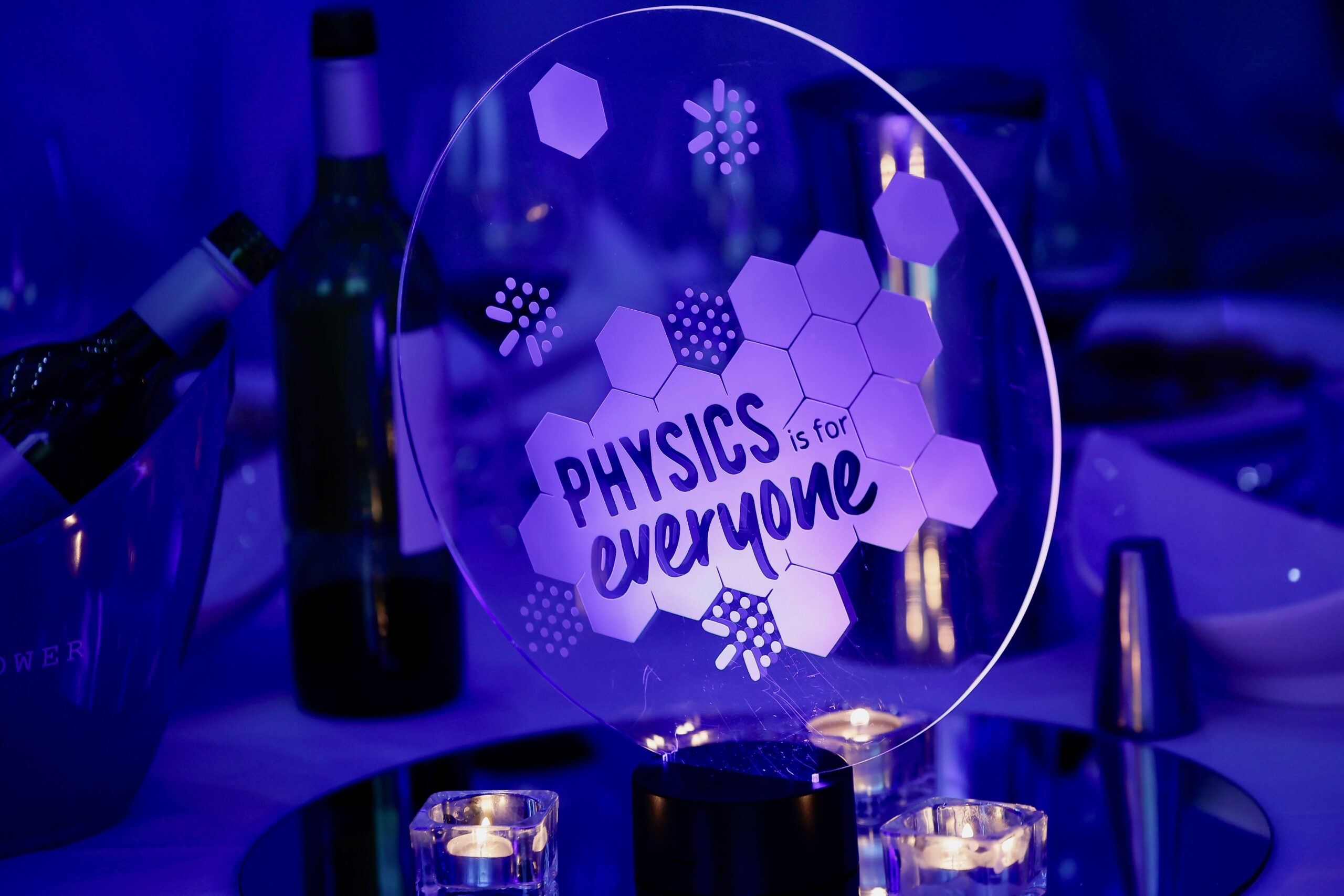
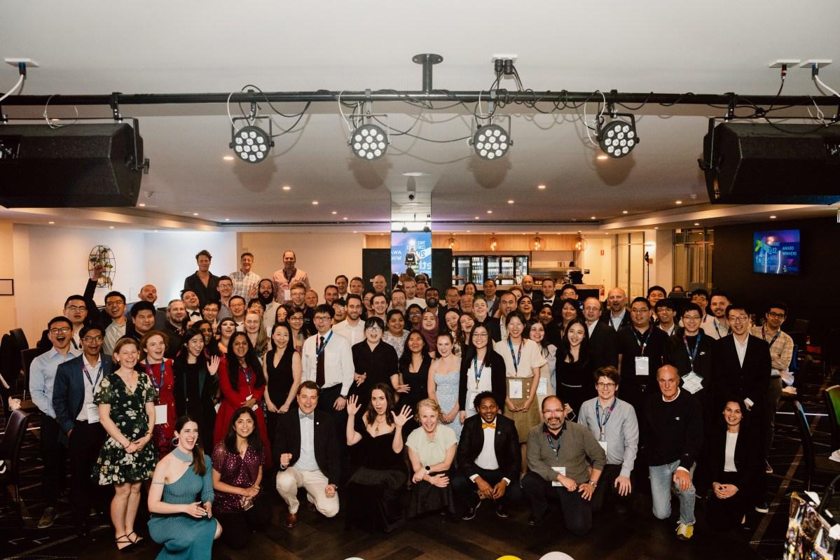
The TMOS Meta Together Conference is here!
About Meta Together
Meta Together is the TMOS annual conference. The purpose of the conference is to connect members of TMOS to share our research and encourage collaboration and engagement across the Centre.
The focus of this year’s TMOS conference will be on collaboration: between TMOS nodes, with end-users/industry, and/or with Partner Investigators (PIs).
Who should attend Meta Together 2025?
Meta-Together 2025 is open to members and guests of TMOS.
Who can present at Meta Together 2025?
Special Tutorial Talks (60 minutes): presented by invited speakers.
Contributed Student Talks (15 minutes): Open to PhD students.
Posters: PhD students and Early Career Researchers (ECRs) can present their work in poster format. Nominations must be made by a TMOS Chief Investigator and will be reviewed and selected by the conference committee.
Meta Shark Tank 2025: A dynamic session where participants pitch innovative ideas to a panel of experts.
Invited Tutorial Speakers
We are delighted to announce that our conference will be visited by:
 Professor Hannah Joyce
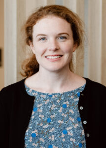 Professor Hannah Joyce
Hannah Joyce is Professor of Electronic and Photonic Engineering at the University of Cambridge. She obtained her BSc and BE degrees from the University of Western Australia in 2005 and her PhD from the Australian National University in 2010. She then joined the University of Oxford as a postdoctoral researcher. In 2013, she established her own research group in the Department of Engineering at the University of Cambridge. Her research interests span low-dimensional semiconductor materials, the development of new nanomaterial-enabled optoelectronic systems, and terahertz photonics. She is the recipient of an IEEE Photonics Society Young Investigator Award, a Philip Leverhulme Prize in Engineering, an International Symposium on Compound Semiconductors/Compound Semiconductor Week Young Scientist Award, and the Zhenyi Wang Award.
 Professor Andrei Lavrinenko
Andrei Lavrinenko received the Ph. D., and D. Sci. degrees from the Belarusian State University, Minsk, Belarus, in 1989, and 2004, respectively. Since 2004, he has been a Professor with the Department of Electrical and Photonic Engineering, Technical University of Denmark. Since 2008, he has been leading the Metamaterials Group of this department. He is the author of more than 250 journal papers. His research interests include metasurfaces, plasmonics, photonic crystals, and numerical methods in nanophotonics.
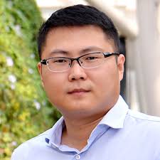
 Professor Yang Chai
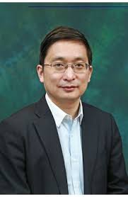 Professor Yang Chai
Prof. Yang Chai is the Chair Professor of Semiconductor Physics of the Hong Kong Polytechnic University. He is an IEEE Distinguished Lecturer, an IEEE Fellow, an Optica Fellow, the Vice President of the Physical Society of Hong Kong, a member of The Hong Kong Young Academy of Sciences, and an Associate Editor of ACS Nano. He is a receipt of the Falling Walls Science Breakthroughs in Engineering and Technology for his work on “Breaking the Wall of Efficient Sensory AI Systems” and the BOCHK Science and Technology Innovation Prize. His current research interest mainly focuses on emerging electronic devices.
Professor Goki Eda
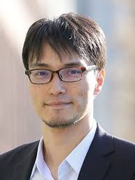
Prof. Goki Eda is an Associate Professor in the Departments of Physics and Chemistry at the National University of Singapore (NUS), specializing in two-dimensional (2D) materials. He earned his M.Sc. from Worcester Polytechnic Institute and his Ph.D. from Rutgers University. After a tenure as a Newton International Fellow at Imperial College London, he joined NUS in 2011. Prof. Eda’s research focuses on the electronic and optical properties of 2D semiconductors, particularly excitons, and their applications in quantum photonics and optoelectronics. He has received several accolades, including the President’s Science and Technology Young Scientist Award (2015) and the University Young Researcher Award (2015). Additionally, he serves as an Associate Editor for npj 2D Materials and Applications. His work continues to influence the development of next-generation electronic and photonic devices.
Professor Weibo Gao
Prof. Weibo Gao is Chair of the School of Electrical & Electronic Engineering at NTU Singapore and holds the Dieter Schwarz Endowed Professorship in Quantum Sovereignty and Resilience (QUASAR). He is also a Professor in the Schools of Electrical & Electronic Engineering and Physical & Mathematical Sciences. Prof. Gao serves as Director of the Centre for Quantum Technologies at NTU (CQT@NTU). His research focuses on quantum technologies using solid-state systems like color centers and 2D materials. These platforms support quantum sensing, communication, and integrated photonic computation. He earned his PhD from the University of Science and Technology of China and was a Marie Curie Fellow at ETH Zurich. He joined NTU in 2014 and became Provost’s Chair Professor in 2019. Prof. Gao has received the President’s Young Scientist Award and the World Scientific Medal. He was also named an MIT Technology Review Innovator Under 35 (Asia). His work strengthens Singapore’s leadership in quantum science and technological resilience.
Professor Hai Son Nguyen

Hai Son Nguyen holds a degree in Physics (2009) from the École Normale Supérieure de Paris and a PhD in Physics (2011) from the Laboratoire Pierre Aigrain (ENS Paris), where he studied single-photon emission from semiconductor quantum dots. From 2011 to 2014, he was a CNRS postdoctoral researcher at the Laboratoire de Photonique et de Nanostructures, focusing on light-matter coupling in nanophotonics. Since 2014, he has been an Associate Professor at ÉcoleCentrale de Lyon and a junior member of the Institut Universitaire de France (2020–2025). In 2024, he received the Fabry de Gramont Prize for his contributions to non-Hermitian photonics and optoelectronic devices. His research at the Institut des Nanotechnologies de Lyon focuses on light-matter interactions in three key areas: optical lattices and metasurfaces, perovskite-based emitting devices, and single-photon emitters for telecom wavelengths.
 Professor Christina Lim
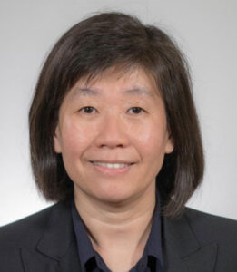 Professor Christina Lim
Christina Lim is an Australian expert on optical wireless communications, radio over fiber, and hybrid “fiber-wireless” networks combining fiber connections to base stations with wireless connections to individual devices. Beyond optical communications, she has also developed transparent displays for augmented reality. She is a professor in the Department of Electrical and Electronic Engineering at the University of Melbourne, where she directs the Photonics and Electronics Research Laboratory. Lim studied electrical and electronic engineering at the University of Melbourne, obtaining a bachelor’s degree in 1995 and completing her Ph.D. in 2000. She has been part of the Photonics Research Laboratory since 1999. Lim was named as an Optica Fellow, in the 2019 class of fellows, “for outstanding and sustained pioneering contributions to the research, development, and applications of fiber-wireless technology in the field of microwave photonics”. She was elected as an IEEE Fellow in 2023, “for contributions in hybrid fiber-wireless communications technology”.
 Professor Mark Brongersma
 Professor Mark Brongersma
Mark Brongersma is a Professor in the Department of Materials Science and Engineering at Stanford University. He received his PhD in Materials Science from the FOM Institute in Amsterdam, The Netherlands, in 1998. From 1998-2001 he was a postdoctoral research fellow at the California Institute of Technology. During this time, he coined the term “Plasmonics” for a new device technology that exploits the unique optical properties of nanoscale metallic structures to route and manipulate light at the nanoscale. His current research is directed towards the development and physical analysis of nanostructured materials that find application in nanoscale electronic and photonic devices. Brongersma received a National Science Foundation Career Award, the Walter J. Gores Award for Excellence in Teaching, the International Raymond and Beverly Sackler Prize in the Physical Sciences (Physics) for his work on plasmonics, and is a Fellow of the Optical Society of America, the SPIE, the American Physical Society, and the Materials Research Society.
This year our invited speakers were asked to present practical tutorials to the community. See below to read abstracts of the tutorials.
Day 1 – Tuesday 18th November 2025
Professor Weibo Gao
A Tunable Entangled Photon-pair Source Based on a Van der Waals Insulator
Scalable quantum photonic devices drive the development of compact sources of entangled photons, which are pivotal for quantum communication, computing, and cryptography. In this work, we present entangled photon pair generation in rhombohedral boron nitride (r-BN), leveraging its unique optical and structural properties. Unlike conventional hexagonal boron nitride, which suffers from reduced nonlinear response due to centrosymmetric structure in even-layered stacks, r-BN features interlayer ABC stacking and maintains robust in-plane inversion symmetry. These characteristics lead to highly efficient entangled photon generation. Our system demonstrates an entangled photon pair generation rate up to 8667 Hz/(mW·mm) and offers a tunable platform for Bell state generation by simply adjusting the pump polarization, without compromising the entanglement quality or generation efficiency. The polarization entangled state is measured with a fidelity up to 94%. This advancement not only marks a significant step towards ultrathin, scalable quantum devices but also establishes r-BN as a promising candidate for on-chip integrated quantum optical applications.
Professor Goki Eda
Exciton Photonics with Atomically Thin Semiconductors
Two-dimensional (2D) van der Waals semiconductors such as monolayer MoS₂ and WSe₂ have emerged as versatile building blocks for photonic devices, owing to their strong excitonic resonances and rich many-body physics. In this tutorial-style talk, I will trace the development of exciton photonics with 2D semiconductors – from the discovery of their fundamental optical properties to recent advances in device integration and quantum light sources. I will then highlight a few recent directions from our group: the observation of an unusual upconversion electroluminescence phenomenon in plasmonic tunnel junctions [1]; and single-photon emission from impurity-bound excitons in substitutionally doped monolayers [2]. These examples illustrate how coupling excitonic materials with nanoscale architectures and precise chemical engineering can open new avenues for optoelectronic and quantum photonic applications. I will conclude with a brief outlook, pointing to symmetry engineering and interfacial ferroelectricity as emerging degrees of freedom that may further expand the potential of 2D semiconductors for novel applications.
[1] Wang et al. “Upconversion electroluminescence in 2D semiconductors integrated with plasmonic tunnel junctions” Nature Nanotech. (2024)
[2] Loh et al. “Nb impurity-bound excitons as quantum emitters in monolayer WS2” Nature Comm. 15, 10035 (2024)
James Liddle-Wesolowski
Creation of Room Temperature Spin Active Quantum Emitters in Hexagonal Boron Nitride
Hexagonal boron nitride (hBN) is a two-dimensional Van der Waals material that can be treated to host quantum emitters. Furthermore, the discovery of a narrowband spin active emitter in hBN increases the materials potential for quantum sensing. This work covers the generation of visible emitters though annealing and emitter characterisation for spin analysis. Finding a reliable method to generate the spin active emitters at a high density would increase the number of emitters for characterisation, subsequently aiding the process of identifying spin active emitters. The emitter characterisation was performed on a confocal microscope, with the capability to record a photoluminescence (PL) map for identifying the spatial position of emitters along with the emitter density. The set-up was also connected to a spectrometer revealing information about the emitters zero-phonon line (ZPL). To determine if the generated emitters have quantum properties the second order correlation was measured. This work performed a comparison between undoped hBN and carbon doped hBN (c-hBN) finding the presence of carbon results in emitters with ZPLs at a longer wavelength and an increased rate of detecting spin active emitters. These results provide groundwork for the use of hBN visible quantum emitters in quantum sensing.
Day 2 – Wednesday 19th November 2025
Professor Hannah Joyce
THz Photonics and Related Applications
Dr. Gurpreet Singh
Spectral Reconstruction of MEMS Fabry–Pérot Filter
Spectral reconstruction is a technique used to estimate the full spectral response of a device from a limited set of available information. It will allow us to examine the device response without requiring an expensive and specialised set of equipment. This can be achieved utilising various algorithms such as prior-based methods and/or data-driven deep learning approaches. Spectral reconstruction of a device becomes even critical where the response of the device exceeds the instrument’s capabilities. This allows us to determine the true response of a device, rather than limiting it due to instrument resolution.
In this work, we are using the microelectromechanical systems (MEMS) based Fabry–Pérot filters (FPFs) [1-3] to validate the concepts. These MEMS-based FPFs were designed and fabricated at the University of Western Australia (UWA) in a microelectronics standard clean environment. The spectral response of these devices is also measured at UWA using a monochromator with a resolution exceeding that of the device. To validate the device response using data reconstruction, the device response is recorded under the broadband light using basic electronics instruments, such as a lock-in amplifier. The data reconstruction will be performed at the University of Melbourne. The preliminary work has started to achieve the desired outcome. We are looking forward to presenting a preliminary proof-of-concept for the data reconstruction of MEMS-based FPFs for the passband wavelength ranging from 1.3 to 1.6 μm.
[1] Optical Microelectromechanical Systems Technologies for Spectrally Adaptive Sensing and Imaging, Advanced Functional Materials, Vol. 32, No. 3, 2103153, 14.01.2022.
[2] Investigation of MEMS-based spectrally adaptive Fabry-Pérot interferometers for long-wave infrared applications, Research output: Doctoral Thesis
[3] Large Area Silicon-Air-Silicon DBRs for Infrared Filter Applications, J. Lightwave Technol. 37, 769-779 (2019)
Ziwei Yang
Dual-Wavelength Multifunctional Metalenses in Mono-Crystalline Silicon Carbide for Quantum Emission Collection
Silicon carbide (SiC) has attained increased attention over the last decade due to its attractive optical properties, including a low loss in the visible and infrared spectrum, strong optical nonlinearity, and the presence of room-temperature quantum emitters [1]. To increase the collection efficiency of such emitters, the conventional solid immersion lenses can be replaced by monolithic metalenses, as demonstrated for diamond-based quantum emitters [2]. Recently mono-crystalline SiC metalenses have also been realized [3], confirming the feasibility of this approach. However, these demonstrations remain limited in functionality, typically operating at a single wavelength and for a single optical task. Extending SiC metalenses to multifunctional free-space operation—such as multi-wavelength collection and polarization-resolved emission control at different angles—has not yet been achieved, despite its importance for versatile next-generation quantum photonic applications.
In this work, we design and demonstrate a pair of multifunctional monolithic SiC metalenses, one operating at 860 nm and the other at 1240 nm, each capable of directing different polarizations to distinct focal positions. The 860 nm metalens targets emission from negative silicon monovacancy in 4H-SiC. These defects serve as optically addressable spin qubit applications, making them highly attractive for quantum technologies and scalable quantum photonic platforms [4]. The 1240 nm metalens collects emission near to the common defects in the 4H-SiC, whose zero-phonon line lies in the telecom O-band and is highly desirable for quantum communication and fiber-based networks. Both devices exhibit robust performance, efficiently capturing emissions from quantum emitters embedded near the surface of mono-crystalline SiC, and demonstrate the potential of multifunctional SiC metalenses as scalable building blocks for integrated and free-space quantum photonic platforms.
[1] Room temperature coherent control of defect spin qubits in SiC, Nature 479, 84 (2011).
[2] A monolithic immersion metalens for imaging solid-state quantum emitters, Nat. Commun. 10, 2392 (2019).
[3] Monolithic silicon carbide metalenses. ACS Photonics 9.4 (2022): 1409-1414.
[4] High-fidelity spin and optical control of single silicon-vacancy centres in silicon carbide. Nature communications 10.1 (2019): 1954.
Joshua Jordaan
III-V Metasurface Lasers for Compact and Directional NIR Emission
Planar metasurfaces provide a compact platform for laser cavities and output couplers, combining subwavelength modal control with wafer-scale fabrication and seamless integration with diverse gain media [1], [2]. By tailoring the unit-cell geometry and exploiting symmetry, metasurfaces can support resonances with long radiative lifetimes while maintaining free-space addressability. These modes enable strong field confinement, narrow linewidths, and efficient vertical emission. Recent demonstrations have shown devices consisting of dielectric metasurfaces, coated with gain media cladding after patterning, that lase into high-Q, dispersionless modes [3], [4]. Such flat-band resonances enhance light-matter interaction through suppressed group velocity and increased density of states, offering opportunities for collective and nonlinear effects in nanophotonic light sources.
In this work, we report the characterisation of near-infrared (NIR) metasurface lasers patterned directly on epitaxially lifted-off III-V semiconductor membranes. The devices are optimised to exploit flat-band modal engineering for efficient lasing. Epitaxial lift-off (ELO) decouples the active III-V gain stack from the growth substrate, enabling wafer reuse and transfer onto low-index transparent hosts. This configuration enhances index contrast for stronger confinement and permits backside optical pumping through the substrate, simplifying integration, packaging, and scalability of compact metasurface-based lasers.
[1] S. T. Ha et al., ‘Directional lasing in resonant semiconductor nanoantenna arrays’, Nature Nanotech, vol. 13, no. 11, pp. 1042–1047, Nov. 2018, doi: 10.1038/s41565-018-0245-5.
[2] D. Wen and K. B. Crozier, ‘Metasurfaces 2.0: Laser-integrated and with vector field control’, APL Photonics, vol. 6, no. 8, p. 080902, Aug. 2021, doi: 10.1063/5.0057904.
[3] S. Eyvazi, E. A. Mamonov, R. Heilmann, J. Cuerda, and P. Törmä, ‘Flat-Band Lasing in Silicon Waveguide-Integrated Metasurfaces’, ACS Photonics, vol. 12, no. 3, pp. 1570–1578, Mar. 2025, doi: 10.1021/acsphotonics.4c02332.
[4] T. T. H. Do et al., ‘Room-Temperature Lasing at Flatband Bound States in the Continuum’, ACS Nano, vol. 19, no. 20, pp. 19287–19296, May 2025, doi: 10.1021/acsnano.5c01972.
Professor Christina Lim
Radio-over-Fibre Technology
Professor Yang Chai
Bioinspired In-Sensor Computing for Artificial Vision
The demand for accurate perception of the physical world leads to a dramatic increase in sensory nodes. However, the transmission of massive and unstructured sensory data from sensors to computing units poses great challenges in terms of power‐efficiency, transmission bandwidth, data storage, time latency, and security. To efficiently process massive sensory data, it is crucial to achieve data compression and structuring at the sensory terminals. In‐sensor computing integrates perception, memory, and processing functions within sensors, enabling sensory terminals to perform data compression and data structuring. In this talk, I will describe our team’s efforts towards bioinspired in-sensor computing for artificial vision. I will talk about the framework of the in-sensor computing and demonstrate a few vision sensors for different scenarios, including visual adaptation, motion perception, as well as event-driven vision sensors for spiking neural network.
References
[1] Nature Electronics, 2022, 5, 84-91
[2] Nature, 2022, 602, 364
[3] Nature Electronics, 2020, 3, 664-671
[4] Nature, 2020, 579, 32-33
[5] Nature Nanotechnology, 2019, 14, 776-782
[6] Nature Electronics, 2022, 5, 483-484
[7] Nature Nanotechnology, 2023, 18, 882-888
[8] Nature Electronics, 2023, 6, 870-878
[9] Nature Nanotechnology, 2024, 19, 919-930
[10] Nature Electronics, 2024, 7, 705-713
[11] Nature Electronics, 2025, 8, 147-156
[12] Nature Electronics, 2025, 8, 680-688.
Dr. Jiajun Meng
Design and Demonstration of Polarisation – Resolved Ge Metalenses for MWIR Imaging
Emerging optical components based on metamaterials and metasurfaces, particularly metalenses, are
transforming conventional infrared (IR) imaging systems by offering compact, lightweight, and cost-effective
alternatives to bulky refractive optics. Traditional IR lenses are typically expensive and heavy, limiting their
use in drones, handheld devices, and wearable imaging platforms. Here, we report the design, modelling,
fabrication, and demonstration of flat mid-wave infrared (MWIR) metalenses based on ultra-thin germanium (Ge) pillars on a silicon (Si) substrate, optimised for operation at 3.3 µm wavelength. In addition to a conventional design, we explore a polarisation-sensitive configuration that enables polarisation splitting,
providing spatially-resolved polarisation contrast and opening pathways for enhanced imaging modalities in
the MWIR.
Numerical modelling efforts, including rigorous coupled-wave analysis (RCWA), were used to construct a
pillar-based phase library and guide metalens performance optimisation. Two types of Ge metalenses were
fabricated: (i) a polarisation-insensitive version using circular pillars (1.5 mm aperture, 4 mm focal length),
and (ii) a polarisation-sensitive version using rectangular pillars for dual-spot focusing (1.5 mm aperture, 3
mm focal length). A subwavelength pillar pitch of 1.1 µm was selected to suppress higher-order diffraction
losses while keeping the fabrication process practical. Infrared imaging tests were performed using FLIR
Lepton uncooled microbolometer arrays with heat sources (e.g., HPIR103). Fabrication quality was confirmed via SEM imaging; incomplete etching (~0.42 µm) degraded imaging contrast, whereas fully etched structures (~1.35 µm) produced significantly improved performance. The polarisation-sensitive metalens demonstrates polarisation-resolved MWIR imaging, offering additional contrast mechanisms and sensing capabilities beyond conventional intensity-based imaging. This study highlights the feasibility of MWIR imaging with flat metalenses and underscores their strong potential for scalable, wafer-level, batch-compatible manufacturing.
The approach is readily extendable to the long-wave infrared (LWIR) regime, paving the way for compact,
lightweight, and mass-producible infrared imaging systems across multiple spectral bands.
Day 3 – Thursday 20th November 2025
Professor Hai Son Nguyen
Engineering Flatbands and Unidirectional Emission in Bilayer Photonic Metasurfaces
Yang Yu
Indium Arsenide Nanowire Array Based Spectrometer for Extended-SWIR Applications
The short-wave infrared (SWIR) wavelengths (1–3 μm), characterized by strong molecular absorption features and low scattering loss, is critical for advanced applications in biomedical imaging, environmental sensing, and industrial monitoring. Traditional spectroscopy in this range relies on bulky and expensive Fourier transform infrared (FTIR) systems, which often requiring cryogenic cooling and thereby limits their integration into compact and portable systems.
In this work, we present a high-performance, filter-free SWIR photodetector and on-chip spectrometer based on InAs/InP/ITO radial p–n heterojunction nanowire (NW) arrays. By incorporating a strain-relieving, double-graded InAsP buffer and a thin InP shell passivation layer, we grow high-quality p-type InAs NW arrays with large, tunable diameters on lattice-mismatched p-type InP substrates using selective area metal-organic chemical vapor deposition. The resulting devices exhibit broadband SWIR photodetection from 1 to 3.3 μm at room temperature. Our photodetectors deliver excellent performance, with peak responsivity up to 0.25 A/W at room temperature (and 0.38 A/W at 150 K), detectivity up to 2.43×10⁹ (300 K) and 1.81×10¹¹ cm·Hz1/2/W (150 K), and high-speed modulation beyond 60 kHz. By tailoring the NW array geometry, we realize wavelength-tunable photodetection across the extended-SWIR (eSWIR) band (1500–2700 nm), all grown on the substrate from the same epitaxial growth. High resolution (305×305 pixels) multispectral imaging is also demonstrated under white light, 1550 nm, and 2200 nm illumination.
Furthermore, by integrating 16 spectrally distinct photodetector arrays onto a single chip with each array functioning as a narrowband pixel with tailored responsivity, and using computational reconstruction algorithms, we demonstrate broadband spectrometry from 1 to 3 μm with a spectral resolution of ~7 nm. As a proof of concept, we reconstruct the transmission spectrum of water and resolve key absorption peaks at 1685 nm and 2210 nm, highlighting the platform’s potential for compact, chip-scale material identification and environmental sensing in the SWIR domain.
Dawei Liu
Broadband Miniature Computational Spectrometer with a Vortex Retarder
Optical spectrometers are essential for studying light-matter interactions, but traditional designs are often complex and bulky. Recent advancements have focused on miniaturized spectrometers for compact and cost-effective applications, relying on recalibrated response functions of nanophotonic structures [1-4]. However, these techniques require precise design and fabrication, posing challenges in balancing size reduction with performance. Here, we introduce an ultra-broadband miniature computational spectrometer using a q-plate vortex retarder between crossed polarizers. The q-plate generates spatially varying birefringence, creating distinctive intensity patterns under different wavelength light, which are captured by a complementary metal oxide semiconductor (CMOS) camera. We use artificial intelligence to extract features from the captured intensity patterns, with spectral reconstruction achieved using Gaussian basis functions and regularization techniques. This enables high-resolution spectral measurements across a broad wavelength range from 400 nm to 1500 nm with sub-nanometre accuracy. Our spectrometer demonstrates a spectral peak location accuracy better than 1 nm and can resolve peaks separated by 3 nm in a bimodal spectrum. This compact design offers a scalable and high-performance solution for miniature optical spectrometers. It is suitable for various fields, including environmental monitoring and biomedical imaging. The integration of advanced computational techniques and novel materials ensures robust and reliable spectral data analysis, reducing the need for precise component alignment and extensive calibration.
[1] Deng, W., et.al. Electrically tunable two-dimensional heterojunctions for miniaturized near-infrared spectrometers. Nature Communications, 2022. 13(1), p.4627.
[2] Uddin, M.G. et.al. Broadband miniaturized spectrometers with a van der Waals tunnel diode. Nature Communications, 2024.15(1), p.571.
[3] Yuan, S, et. al. A wavelength-scale black phosphorus spectrometer. Nature Photonics, 2021. 15(8), pp.601-607.
[4] Yoon, H.H., et. al.. Miniaturized spectrometers with a tunable van der Waals junction. Science, 2022. 378(6617), pp.296-299.
Lincoln Clark
Infrared to Visible Image Processing by a Nonlinear LiNbO3 Metasurface
Using Structured Light
Image processing techniques play a critical role in emerging technologies such as autonomous driving, biometric verification, and AR/VR systems [1]. These computation tasks have been performed using digital computers, but the growing demand for speed, power efficiency, and real-time performance is driving innovation beyond conventional architectures. In the IR wavelength regime, image processing using night vision cameras is more complex due to weak signals and the difficulty in extracting fine details [2]. While direct light-to-light conversion via nonlinear processes like sum-frequency generation (SFG) has been used for image conversion, it has not yet been applied to optical image processing. GaAs and LiNbO3 metasurfaces have demonstrated efficient direct light-to-light conversion with promising imaging performance [3, 4]. However, these methods focused solely on wavelength conversion, not on optical image processing. In this work, we perform IR to visible image processing using a nonlocal LiNbO3 metasurface and vortex mirrors with topological charges of 0, 1 and 2 (Fig 1. a).
We compare the processed images with those from the case of charge 0, that corresponds to the standard mirror, serving as a control reference (Fig 1. b). Our results open new opportunities for imaging of transparent biological objects, advanced security systems, and autonomous navigation.
1. Jing, J., Liu, S., Wang, G., Zhang, W. & Sun, C. Recent advances on image edge detection: A comprehensive review. Neurocomputing 503, 259–271. ISSN: 0925-2312 (2022).
2. Ashiba, H. I. & Ashiba, M. I. Super-efficient enhancement algorithm for infrared night vision imaging system. Multimedia Tools and Applications 80, 9721–9747. ISSN: 1573-7721 (2021).
3. Morales, M. C. et al. Infrared imaging in nonlinear GaAs metasurfaces in Proc.SPIE 11201 (Dec. 2019),
112011S.
4. Valencia Molina, L. et al. Enhanced Infrared Vision by Nonlinear Up-Conversion in Nonlocal Metasurfaces. Advanced Materials 36, 2402777 (2024).
Prof. Lan Fu and Prof. Milos Toth
From Research to Reality: What Comes Next beyond TMOS?
Panel speakers:
Prof. Michael Johnston (University of Oxford, TMOS PI)
Prof. Ilya Shadrivov (CI, TMOS)
A/Prof. Noushin Nasiri (Macquarie University)
Dr. Nima Sefidmooye Azar (University of Sydney, Research Fellow, TMOS Alumni)
Dr. Byron Villis (Archer Materials Limited)
Dr. Douglas Little (Department of Nanometrology, National Measurement Institute)
Professor Andrei Lavrinenko
Surface Waves in Photonics
Surface waves typically propagates along an interface of two dissimilar media. In difference with acoustic surface waves, which constitute a base for various devices readily available on the market, photonic surface waves (except surface plasmon-polaritons) are still the topic of the lab research. I will give an overview of a wide variety of surface waves has been investigated in numerous material and structure settings, their excitation and characterization methods and address existing and potential applications.
Dr. Peter Elango
A Compact Optical Sensor to Self-Assess Skin Health After Sun Exposure
Excessive sun exposure is the major environmental risk factor for melanoma and other types of skin cancer.
Reducing cumulative exposure to ultraviolet (UV) radiation and avoiding repeated, sporadic episodes of acute photodamage can drastically lower this risk. Photodamage after sun exposure can be assessed by monitoring erythema – skin redness – and increased pigmentation, both key indicators of excessive UV exposure. In this work, we present a compact optical device designed to monitor changes in pigmentation and erythema through reflectance measurements using four micro-LEDs, emitting at 405 nm, 572 nm, 650 nm and 700 nm and a photodiode with extended visible-NIR sensitivity. Monte Carlo simulations were conducted to optimise the device design by evaluating light penetration into skin tissue as a function of source-to-detector distance to target key chromophores. The device was validated using skin-mimicking tissue phantoms with controlled concentrations of coffee, with similar optical properties to melanin, and haemoglobin to simulate changes in pigmentation and erythema, respectively. Using a signal-to-noise ratio threshold of 2, we were able to detect changes in pigmentation as small as 5% across all phototypes, and erythema changes in lighter skin tones. This miniaturised device shows potential for personalised skin monitoring in therapeutic, cosmetic, and diagnostic applications.
[1] Tang, X., Yang, T., Yu, D., Xiong, H. & Zhang, S. Current insights and future perspectives of
ultraviolet radiation (UV) exposure: Friends and foes to the skin and beyond the skin. Environment
International, 108535 (2024).
[2] McDaniel, D., Farris, P. & Valacchi, G. Atmospheric skin aging—Contributors and inhibitors. Journal
of Cosmetic Dermatology 17, 124–137 (2018).
[3] Brozyna, A. et al. Mechanism of UV-related carcinogenesis and its contribution to nevi/melanoma.
Expert Review of Dermatology 2, 451–469 (2007).
![]()
Day 4 – Friday 21st November 2025
Professor Mark Brongersma
Travel Information
Conference Venue
The conference will be held at the Coogee Bay Hotel, located at 9 Vicar Street, Coogee, New South Wales, 2034.
Established in 1873, the Coogee Bay Hotel has been a central part of the Coogee community for over 150 years. Originally a school in the 1860s, it was transformed into a hotel that quickly became a beloved seaside retreat. Its spacious, sunlit gardens made it a popular destination in the 1920s when Coogee was celebrated as ‘Australia’s most beautiful seaside resort.’ Today, the hotel continues to serve as a cornerstone of the community, offering modern amenities while preserving its rich heritage.
Getting There
The Coogee Bay Hotel is located approximately 14 km from Sydney Airport. Depending on traffic conditions, travel time can range from 20 to 35 minutes.
Taxi: Fares from Sydney Airport to Coogee typically range between AU$32 and AU$60, depending on traffic and time of day. Note that a $5.45 airport toll applies to all taxi departures from the airport. Total travel time is approximately 30 minutes
Uber: Uber fares are generally competitive, often ranging from AU$30 to AU$50 for the trip to Coogee. Uber pickups are available at designated rideshare pickup zones at the airport.
Train & Bus: Take the Airport Link train from Sydney Airport to Central Station. The fare is approximately AU$17.70. From Central Station, you can transfer to Bus Route 370 towards Coogee Beach, which stops near the Coogee Bay Hotel. The bus fare is around AU$4. Total travel time is approximately 45 to 60 minutes, depending on wait times and traffic.
Onsite parking
Parking at our venue is bookable in advance only and is subject to availability.
A limited number of parking spots are available at the conference venue for attendees.
If you’d like to reserve a spot, please register by 03 October 2025.
Parking is charged at $30 per vehicle per day (cars, motorbikes, and scooters included).
⚠️ Please note: Parking cannot be arranged on the day — all bookings must be made in advance. We recommend securing your spot early.
Shark Tank at Meta
Exciting news! At this year’s Meta Together Conference we’re launching something new… TMOS Shark Tank!
We’re inviting PhD candidates and Early Career Researchers to pitch their coolest ideas—be it a clever gadget, an outreach tool, a research translation concept, or something entirely unexpected.
The Winning Team will get $20,000, while the Runner-up Team will get $10,000 to bring their idea to life within 12 months.
Please note: Prize money is allocated for project funding and is not a personal cash prize.
Why are we doing this? Our goals:
- Foster teamwork and collaboration across nodes,
- Enhance skills in pitching and idea communication,
- Encourage creativity, innovation, and a bit of fun.
What can you pitch?
Pretty much anything! A business idea, a hands-on outreach gizmo, a piece of tech, or even a concept that brings research to real-work impact. During Meta 2025 – each team will have 15 mins to pitch the idea to the sharks. The best pitch wins!
Cross node participation is mandatory, and each team must have between 3-6 participants.
Want to enter?
- Choose a name and a title for your idea/pitch and submit your EOI to Sophia.Aharanovich@uts.edu.au.
- Submit your Expression of Interest (EOI) by the deadline: 31 August 2025.
For eligibility, more information and FAQs, click below:
Suggested Accommodation Options
Please note, all accommodation payments must be done by node CIs according to your university requirements and regulations.
Conference Venue
The conference will be held at the Coogee Bay Boutique Hotel, 9 Vicar Street, Coogee New South Wales 2034. Single rooms or twin share rooms are at the venue. There are only limited pre-booked rooms available.
Family/Shared Apartment Hotel near by
For researchers traveling with families, we pre-booked recommended rooms in Adina Apartment Hotel, 183 Coogee Bay Rd, Coogee NSW 2034. This hotel is located about 3oo m from the main venue. Two-Bedroom Queen or King Apartments are available for shared apartment stay as well. Adina Hotel in Coogee
High Level Budget Hotel We Recommend – 1
Crowne Plaza Sydney Coogee Beach, an IHG Hotel is a recently renovated hotel 200 m away from the conference venue at 242 Arden St, Coogee NSW 2034. The hotel offers 5-star accommodations and with 4.2 stars Google reviews. Please note: the rooms in this hotel are not pre-booked. Crowne Plaza Sydney Coogee Beach
Medium Level Budget Hotel We Recommend – 2
Coogee Sands Hotel and Apartments, is a 4-star hotel located only 5 min walking distance from the conference venue at 161-167 Dolphin St, Coogee NSW 2034 . This hotel has a record 4.3 stars Google reviews and can be a medium budget booking. Please note: the rooms in this hotel are not pre-booked. Coogee Sands
Low Level Budget Hotel We Recommend – 3
If you are looking into low budget options near the conference venue, we recommend checking a Little Coogee Hotel, 272 Clovelly Rd, Coogee NSW 2034. This is a 3-star hotel with 4.1 stars Google reviews located about 15 min walk from the venue. Please note: the rooms in this hotel are not pre-booked. Little Coogee Hotel
Hotel of Your Choice
Sydney is a very touristic city with a lot of hotel options to choose from. You might choose any other hotel in Coogee area or around Sydney and use public transport or Uber to travel to the venue. Ther are also a lot of Airbnb options available.
Registration
Registration includes attendance at the conference, Welcome BBQ Dinner, Trivia Night, Gala Dinner and Awards Night with live band music, all lunches, coffee breaks and social drinks.
By registering for this conference, you agree to the Terms and Conditions.
Presentations
ABSTRACT SUBMISSION GUIDELINES
Important dates
- Conference Registration: 5 June – 6 July 2025
- Shark Tank EOI Submission: 1 May – 31 July 2025 EXTENDED 31 August 2025
- Shark Tank Full Application Submission: 1 May – 30 September 2025
- Presentation Abstracts Submission: 5 June – 31 August 2025
- Poster Abstracts Submission: 5 June – 31 August 2025
Conference program
Conference details for attendees
All delegates have received a link to the official TMOS Meta Together Conference 2025 website, which contains the program, delegate information pack, link to Conference 2025 Slack Channel, and other helpful resources. Check the email sent to you by the conference organisers.
Contact
 Sophia Aharonovich
Professional Staff
University of Technology Sydney
events@tmos.org.au

Liz Micallef
Professional Staff
Australian National University
events@tmos.org.au
Steering Committee
Dragomir Neshev
Centre Director
Australian National University
Igor Aharonovich
Chief Investigator
University of Technology Sydney
Milos Toth
Chief Investigator
University of Technology Sydney
Lan Fu
Chief Investigator
Australian National University
Sophia Aharonovich
Professional Staff
University of Technology Sydney
Galina Shadrivova
Business Manager
Australian National University
Liz Micallef
Professional Staff
Australian National University
Mary Gray
Chief Operations Officer
Australian National University
Local Organising Committee
Igor Aharonovich
Chief Investigator
University of Technology Sydney
Milos Toth
Chief Investigator
University of Technology Sydney
Hossein Alijani
Research Fellow
University of Technology Sydney
Chaohao Chen
Research Fellow
Australian National University
Sophia Aharonovich
Professional Staff
University of Technology Sydney
Sponsorship
We thank OXFORD Instruments for their generous sponsorship and continuous support.
![]()
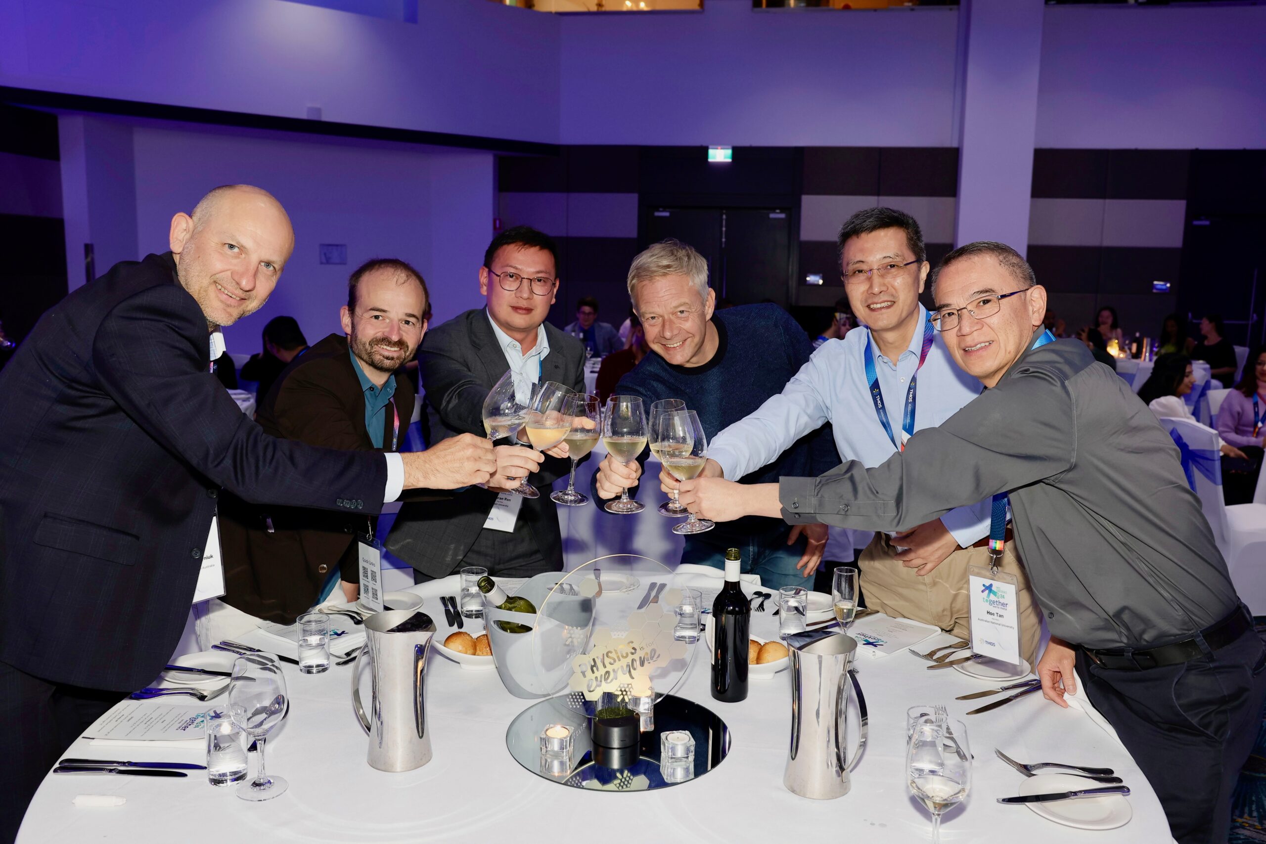
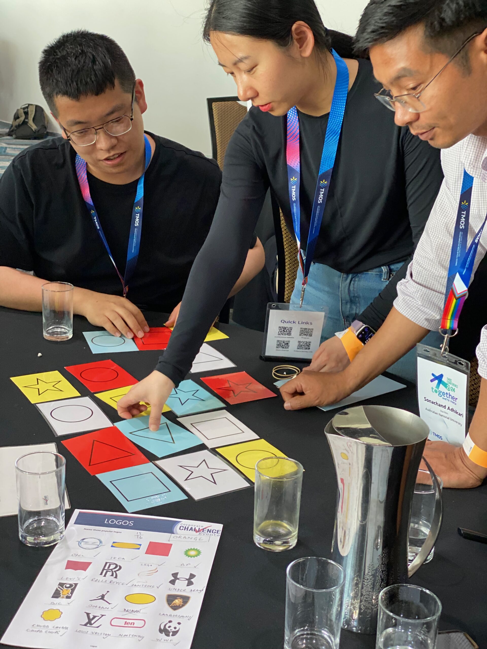
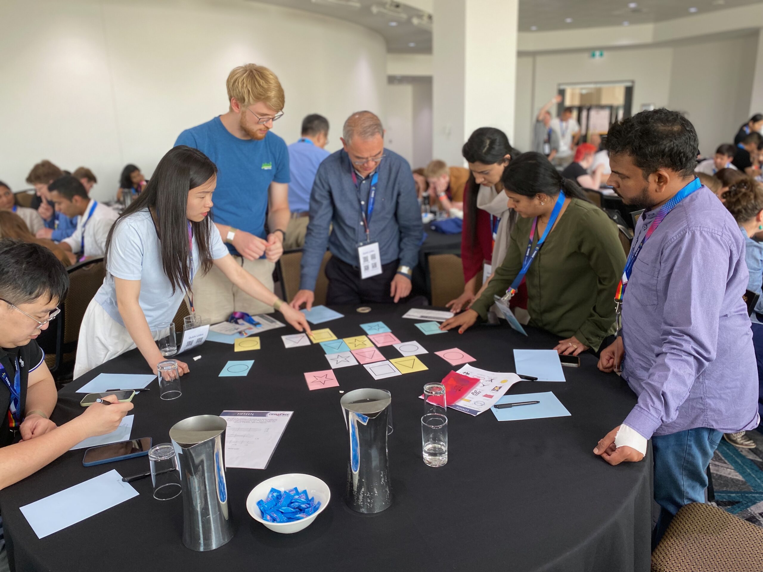
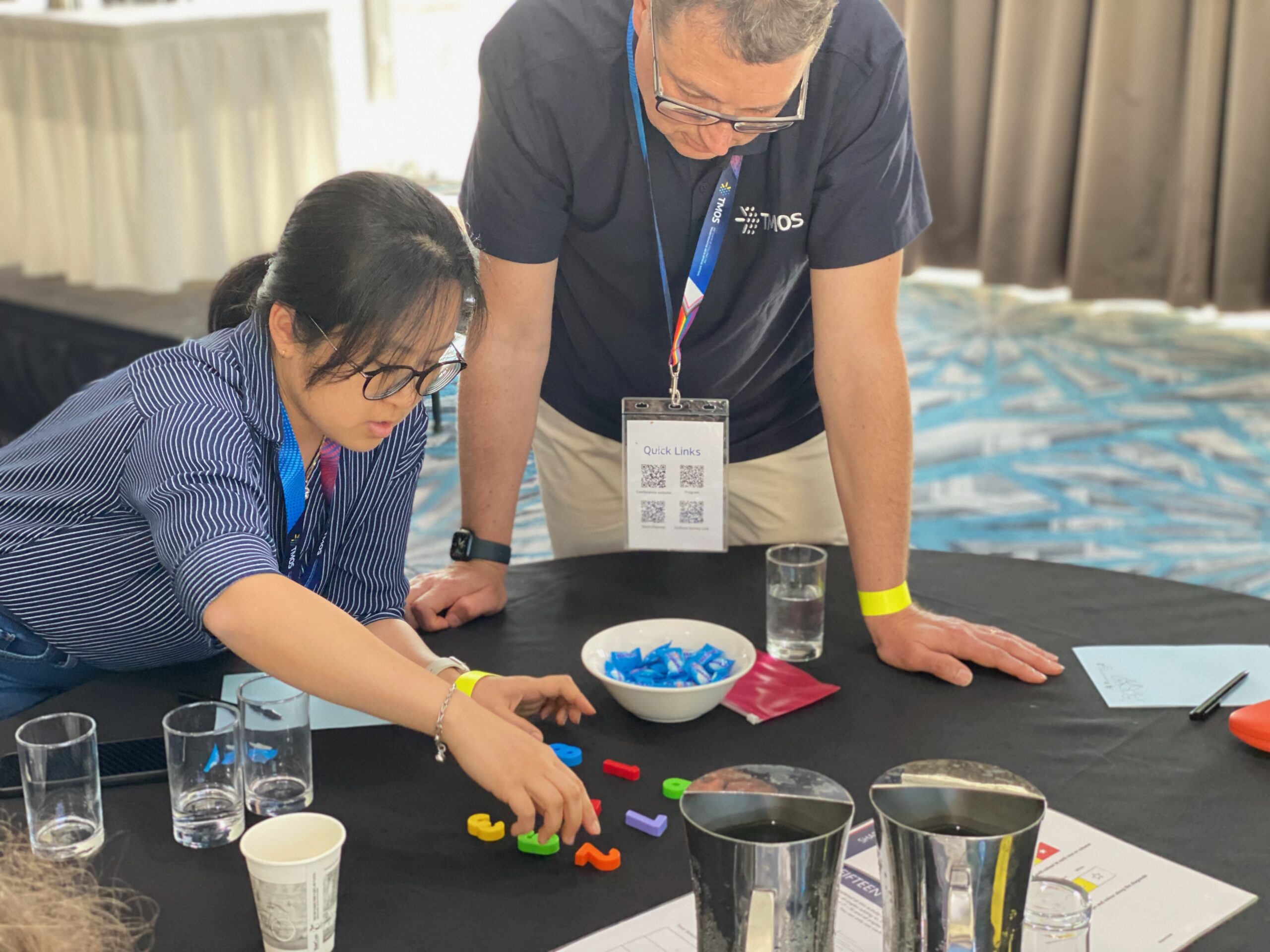
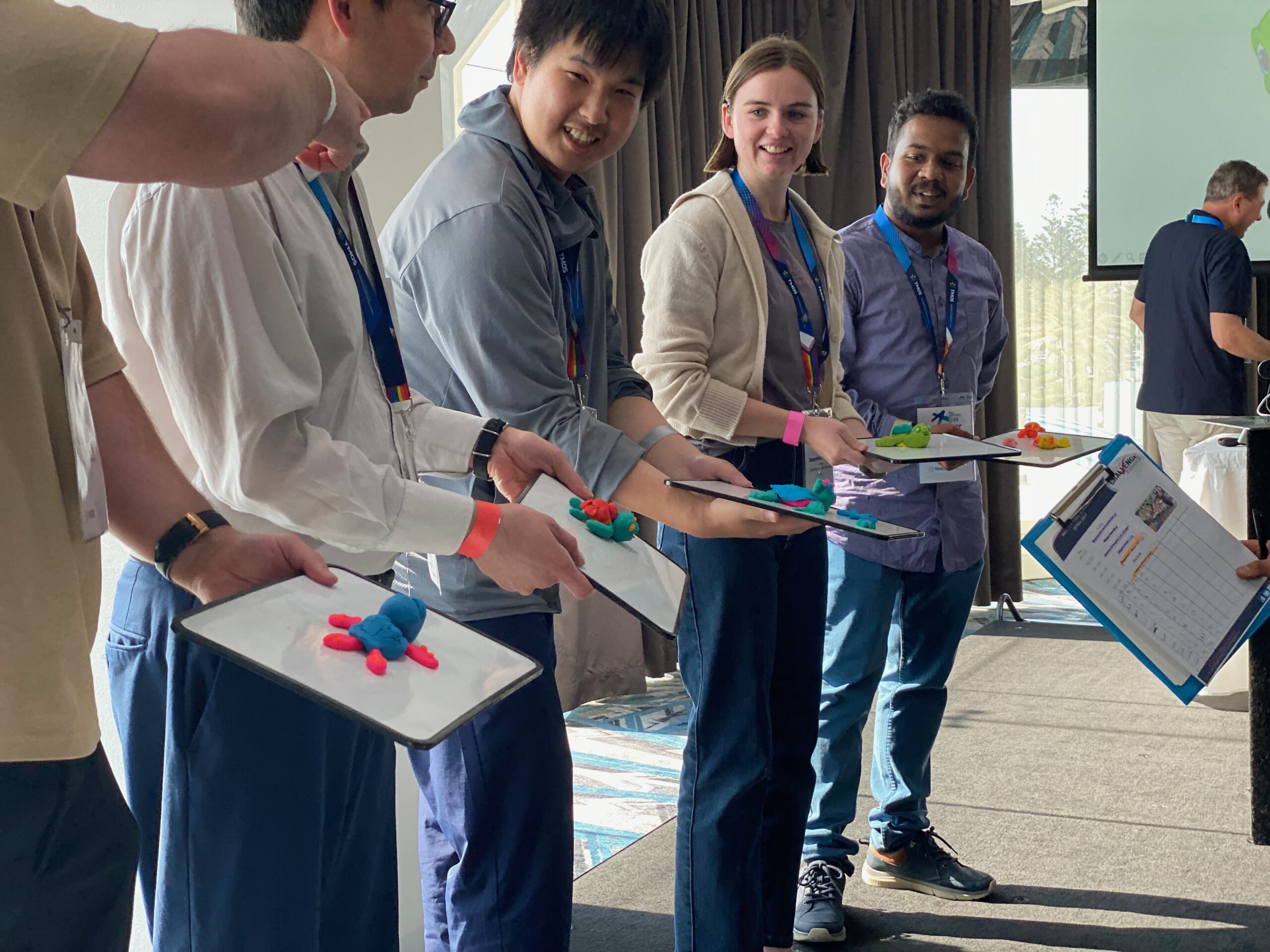
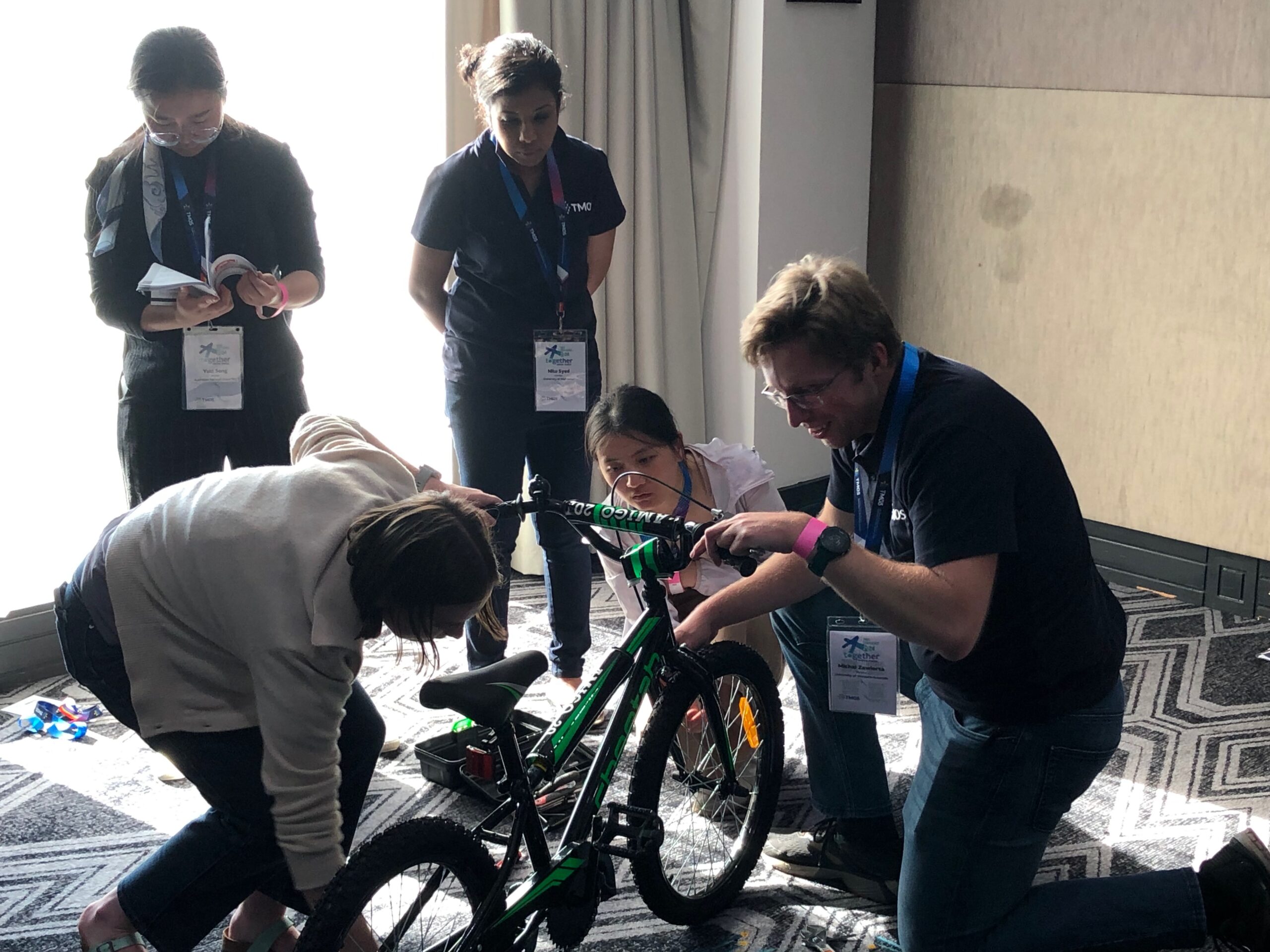
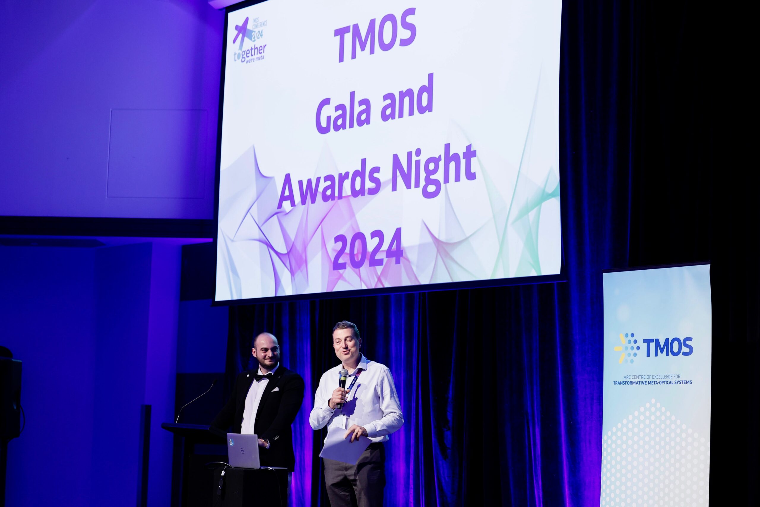
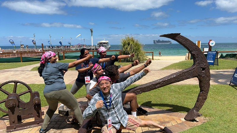
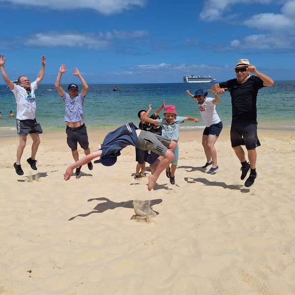
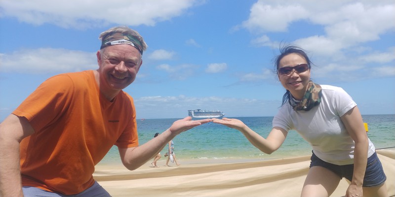
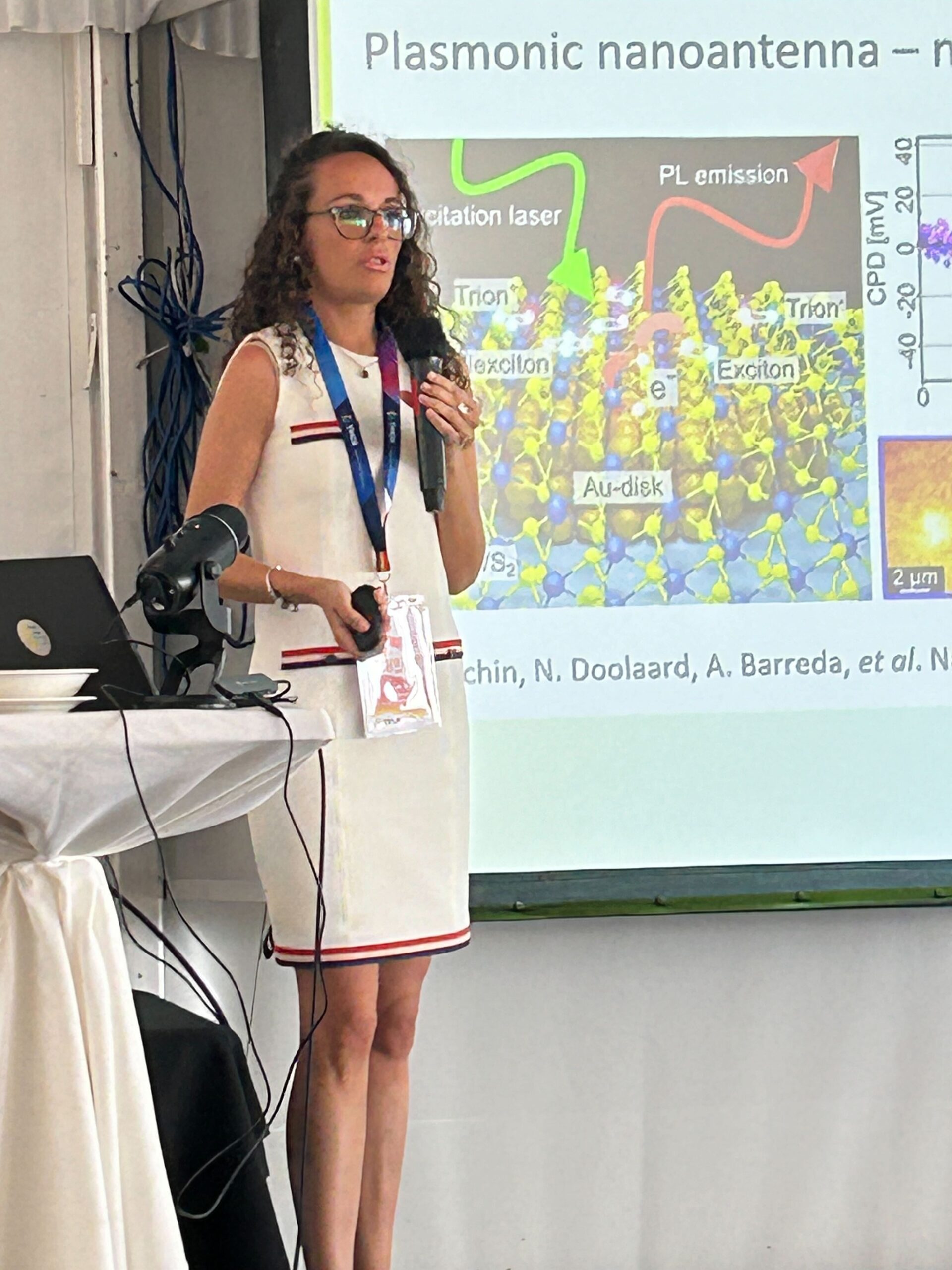
Meta Together 2024
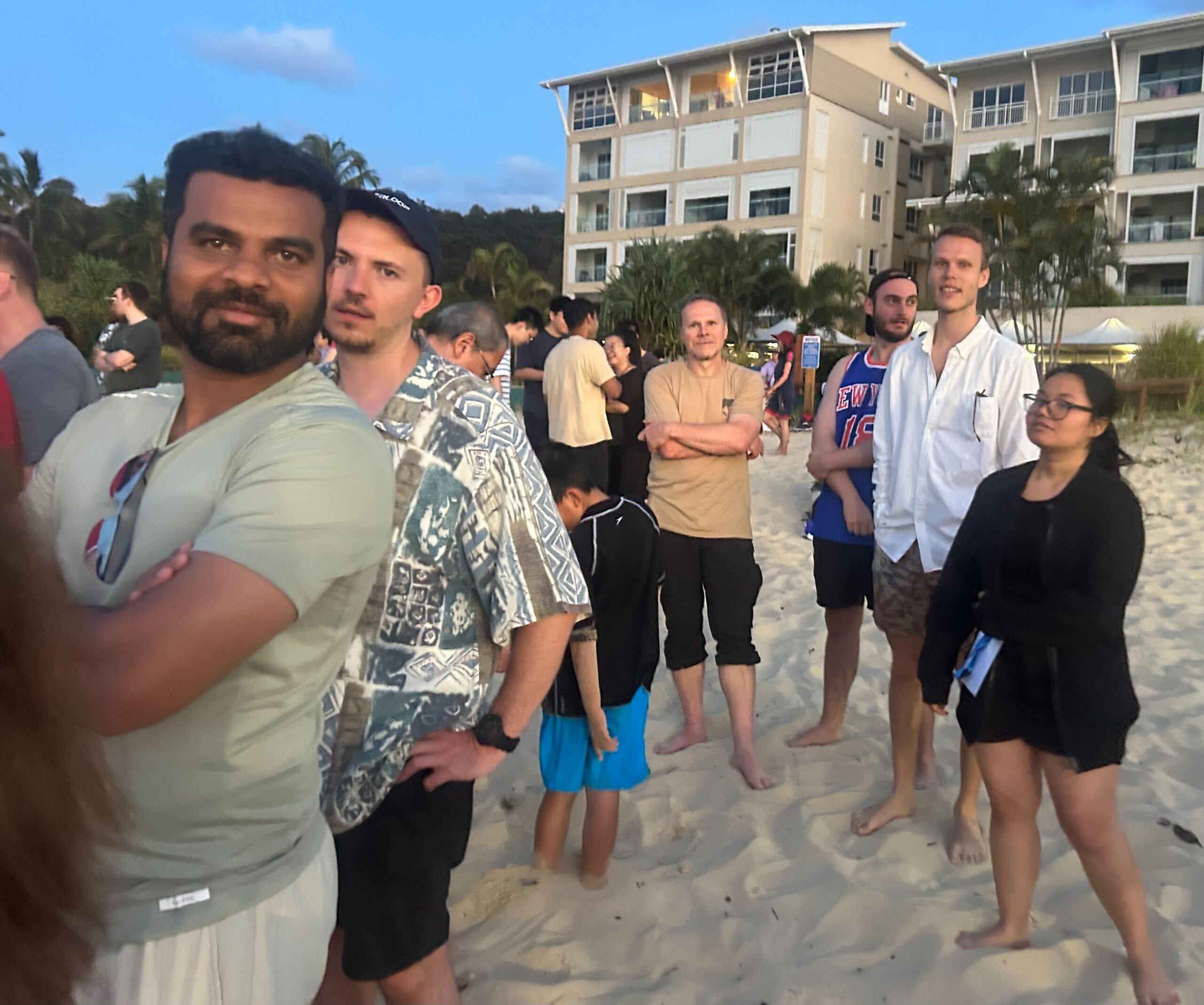
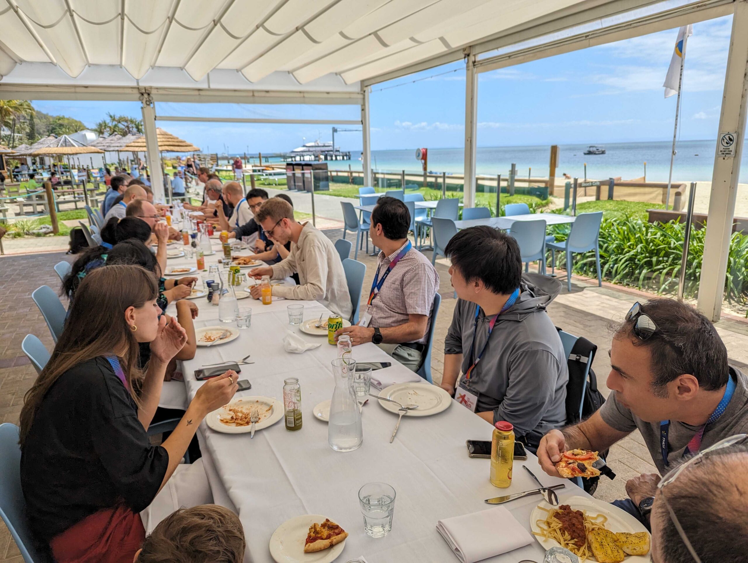
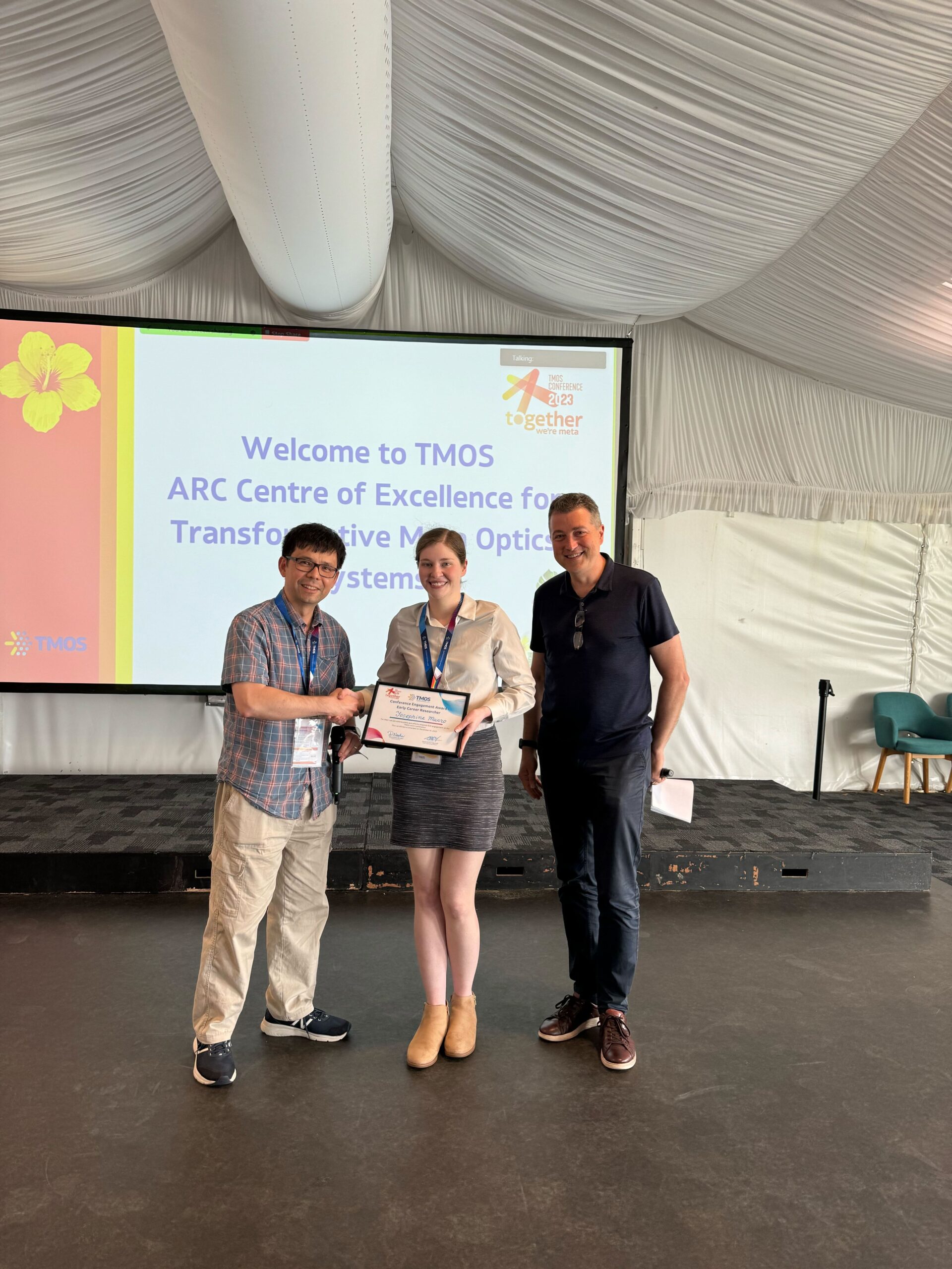
Meta Together 2023
Meta Together 2022
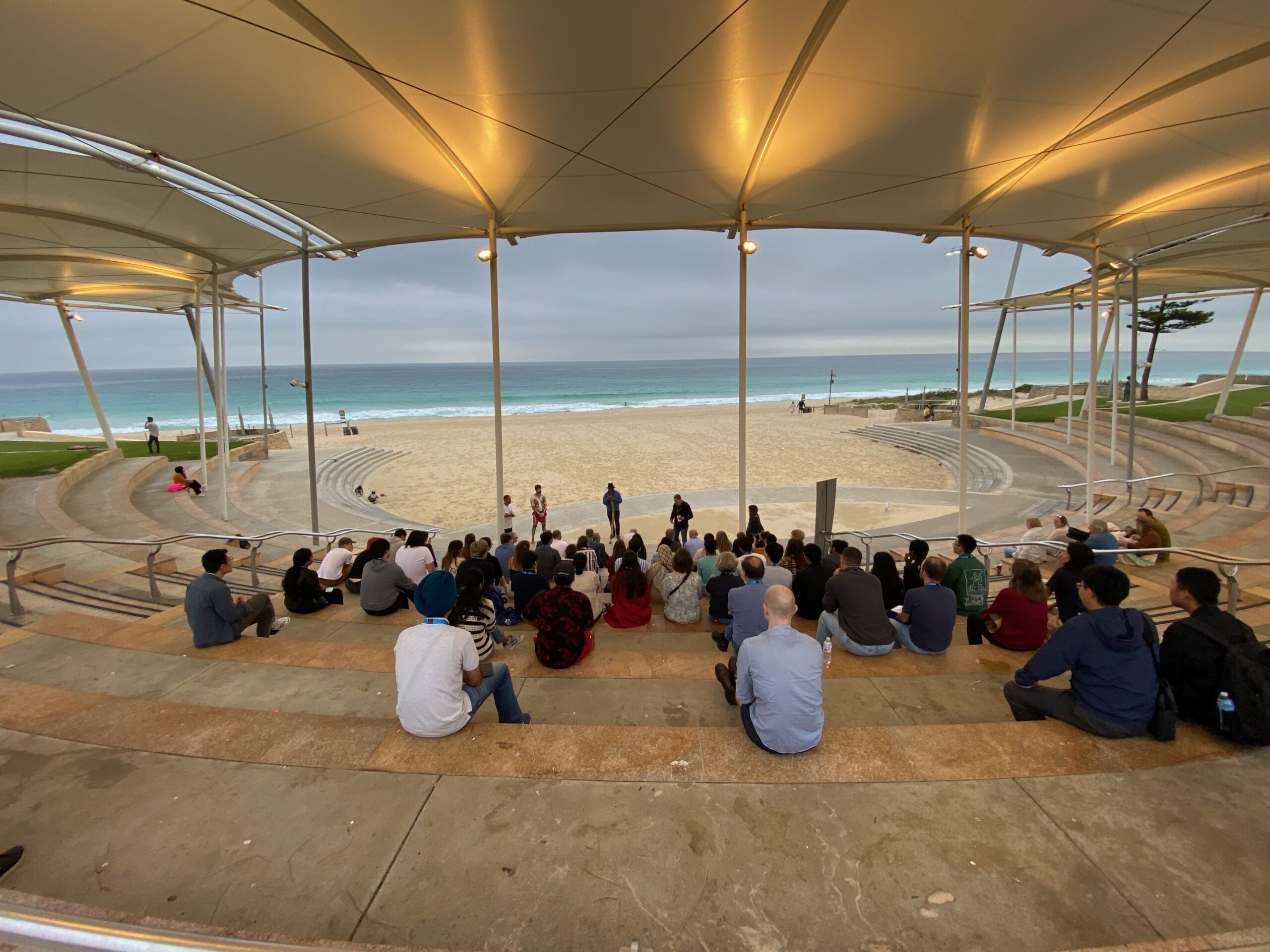
Acknowledgement of Country
The ARC Centre for Transformative Meta-Optical Systems (TMOS) acknowledges the Traditional Owners and their custodianship of the lands on which our teams operate. We pay our respects to their Ancestors and their descendants, who continue cultural and spiritual connections to Country. We recognise their valuable contributions to Australian and global society.