Welcome to Meta-Together 2023! We are excited to have the team together for three days of new research, collaboration, and fun. A PDF of the full program is linked below and beneath that are the abstracts for each research presentation, with links to bios.
Full Meta Together Program
All the information you need regarding travel, accommodation, events etc.
Want to join us virtually?
Don’t miss out on any of the action! You can join us at anytime, from anywhere via Zoom.
Meeting ID: 898 2765 5621 | Password: TMOS2023
Day 1 – Wednesday 13th December 2023

Extreme Control of Light with Metamaterials
The field of metamaterials, artificial engineered materials, has been rapidly evolving in the past two decades, demonstrating extreme optical phenomena and unprecedented control over wave propagation. In this talk, I discuss recent developments in this field of research, with an emphasis on the role of symmetries in establishing emerging optical responses for metamaterials based on otherwise simple constituents. Geometrical rotations, suitably tailored perturbations, and broken time reversal symmetry can be carefully engaged to tailor waves in robust and efficient ways, control their propagation, break Lorentz reciprocity and enable topological order and phase transitions. In particular, the use of strongly coupled light and matter interactions in polaritonic systems enables extreme responses at the nanoscale, well suited for classical-wave and quantum applications. In my talk, I will discuss the underlying physical principles that span over a wide range of frequencies, and their impact on practical technologies, from imaging, energy and sensing to computing and communications.

Nonlinear 2D-material Metasurfaces
In this talk, we would present our recent works on 2D-material-based metasurfaces, which combines the nonlinearity of 2D materials and vdW materials with the artificially structured metasurfaces. We demonstrate the enhanced nonlinear photon emission and further show the wavefront shaping. We also overcome the layer number restriction of the 2D materials, and report the thinnest quantum SPDC light source using a 46 nm vdW crystal. The synergy between low-dimensional materials and metasurfaces holds great potential.

Antimonide based Infrared Avalanche Photodiodes
Photonic infrared detectors have witnessed three generations of development since their first reports in 1950s-60s. The detectors have evolved from single element to linear to large format 2D arrays. In this talk we will discuss a vision for the fourth generation of infrared detectors that incorporate on demand functionality like gain, color, polarization at the pixel level. We will discuss how the advances in metamaterials and photon-absorption enhancing structures could provide a path to addressing some of the technical challenges with in development of these sensors and imaging arrays. We will also discuss the recent interest in 3D imaging for topographic mapping and light detection and ranging (lidar). A low noise linear mode avalanche photodiodes (LmAPDs) is a critically enabling component for eye-safe long range LiDAR and remote sensing applications. Unlike PIN diodes, APDs provide internal gain that can lead to increased signal to noise ratio and suppress downstream circuit noise. The highest performing infrared APDs are based on interband transitions in mercury cadmium telluride (MCT, HgCdTe). Commercial APDs use an InGaAs absorber with an InAlAs or InP multipliers. We are investigating two antimonide based multipliers, AlGaAsSb and AlInAsSb, on InP substrates. We have recently demonstrate GaAsSb/AlGaAsSb separate absorber charge and multiplier (SACM) heterostructures. We will discuss the technical challenges associated with the design, growth, fabrication and test of these LmAPDs and the potential for the development of these critical APD arrays for active 3D sensing and imaging systems.

High Resolution Phase Imaging via Dielectric Metaoptics
Due to the widespread availability of digital cameras, standard image processing involves capturing an image and manipulating it computationally. Prior to the advent of computing, however, image processing operations were performed by optically accessing and filtering spatial frequencies using a 4-f setup [1], necessitating the use of bulky components and propagation distances. Unlike digital approaches, however, these methods permitted access to the phase of an optical field leading to the development of Zernike phase contrast microscopy. Metasurfaces offers a niche opportunity to develop a compact and effective equivalent of optical component in translating phase gradient information into intensity without digital post-processing. However, most existing devices are limited by a relatively low numerical aperture (NA) with an approximately linear optical transfer function (OTF) existing over a narrow range of spatial frequencies, resulting in image artifacts and reduced resolution for microscopic objects [2].
We employed free-form topological optimization via adjoint simulations [3] to design nontrivially shaped silicon nanoresonators on a sapphire substrate (Fig. 1 top middle). This dielectric device demonstrates a nearly linear and asymmetric Optical Transfer Function (OTF) within a numerical aperture of 0.6 in the along the horizontal (x) direction, as depicted in the lower central panel of Fig. 1. This asymmetric response becomes apparent when the device is illuminated with left-circularly polarized (LCP) light and subsequently analyzed using a right-circularly polarized filter at a wavelength of 750 nm.
When phase information (Fig. 1 left) is propagated through the device, the resulting image (Fig. 1 top right) depicts a clear intensity image, highlighting phase gradients in the image, with few artefacts. This result can be compared to an image produced through a device with an asymmetric transfer function across a constrained numerical aperture (NA <0.1) (Fig. 1 bottom right, data reproduced from [4]). It can be observed that the higher NA of the device contributes to improved resolution and prominent reduction in artefacts. Our device potentially provides an alternative to a compact all-optical image processing in the realm of high-resolution phase imaging.
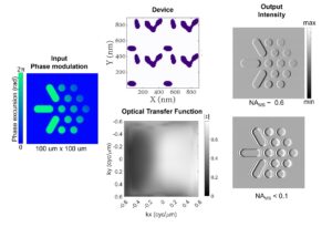
Figure 1: Numerical simulation of image processing through the metasurface. (left) Phase modulation input invisible to standard camera. (middle top) A binary schematic of the 2×2 unit cells of the device showing silicon nanoresonators on a sapphire substrate and (middle bottom) its respective 2-D Optical Transfer Function. (right top) Optically processed intensity image resulting from the propagation of phase modulation input (left) through the device (middle). The resolution of the image increased significantly (NAMS ~ 0.6) compared to the intensity output (right bottom) through a metasurface with a linear transfer function across a narrow spatial frequency range (NAMS < 0.1) [4].
- W. Goodman, Introduction to Fourier Optics, McGraw-Hill (2005).
- Wesemann, T. J. Davis, A. Roberts, Appl. Phys. Rev. 8 (3), 031309 (2021).
- Molesky, Z. Lin, A.Y. Piggott, A.Y. et al. Nature Photonics 12, 659–670 (2018).
- Wesemann, J. Rickett, T. J. Davis, and A. Roberts, ACS Photonics 9 (5), 1803-1807 (2022).

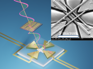
DNA Origami-assisted Unidirectional Transmitting Nanoantennas
Confining the emission of single quantum emitters into a pre-defined direction is of great interest for the applications of single-photon sources. Plasmonic nanoantennas enable the control and manipulation of radiation from single quantum emitters. Previous efforts mostly rely on the interference of coherent waves from multiple resonators [1,2]. The performance depends on the number of resonating elements, making the top-down fabricated unidirectional nanoantennas bulky [1]. Recently, DNA origami technology has been used to produce unidirectional nanoantennas with one emitter and two nanorods [2]. However, further enhancing the directionality by increasing the number of resonant elements would be technically demanding. Here, we demonstrate ultracompact DNA origami-assisted unidirectional nanoantennas (footprint ~ 150 nm) based on Kerker condition, the balanced interference of the induced electric (ED) and magnetic dipole (MD) in the same structure (Fig. 1a). The meta-emitter consists of three gold nanoparticles and a single dye molecule (Atto647N) on a precisely engineered DNA origami template. To bring the emitter to the center of the gap, the DNA origami was designed to capture one of the three gold nanospheres (diameter = ~70 nm) on the opposite side of the triangular origami template (Fig. 1b). Trimer nanoantennas were obtained at high yield (Fig. 1c) and the emission of the single dye molecule show clear unidirectionality. The largest front-to-back emission ratio (F/B) was found to be more than 10 dB (Fig.1d).
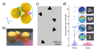
Figure. 1 a) Configuration of the trimer nanoantenna driven by a single emitter (red arrow). The unidirectional radiation pattern (blue contour) stems from the balanced interference of the electric dipole (ED) and magnetic dipole (MD). b) A schematic showing how the curved origami template brings the single emitter to the dimer gap. c) An SEM image of the DNA origami-assisted trimer nanoantennas. d) Representative emission patterns and SEM images of trimer and dimer antennas. Distinct directionality (F/B ratio in dB) is found between trimers (purple dots) and dimers (pink dots).
Anapole and Quasi-bounds states in the continuum modes for enhancing light-matter interaction
Fostering efficient quantum emitters stands as a pivotal pursuit within photonic quantum technologies. Over recent years, there has been an extensive exploration of all-dielectric metasurfaces, driven by the goal of boosting the efficiency of quantum emitters. On the one hand, the directional properties of dielectric nanoparticles have been harnessed to enhance radiation collection [1]. On the other hand, the confinement of electromagnetic energy within the nanoresonators comprising the metasurface has the potential to amplify the emission from electric or magnetic quantum emitters situated within localized hot-spot regions [2]. With the aim to increase light-matter interaction, quasi-bound states in the continuum (q-BIC) resonances can be excited, which are characterized by a high Q-factor [3].
In the case of metasurfaces, symmetry-protected BIC modes are originated due to the mode’s spatial symmetry misaligning with the symmetry of radiating waves. Symmetry breaking in the metasurface facilitates the coupling of the mode’s radiation with incident radiation, thereby giving rise to the q-BIC resonances [3].
Despite the potential for achieving a high Q-factor in all-dielectric metasurfaces, their practical applicability is sometimes constrained by the fixed band emission determined by the design’s geometry. To circumvent this limitation, the incorporation of phase-change materials or liquid crystals has been explored [4].
In this study, we investigate various phase-change materials (Ge2Sb2Te5 and Sb2Se3) to tune the emission of a q-BIC mode within the telecom band. Specifically, we analyze a silicon metasurface comprising two asymmetric nanobars, each featuring a thin layer of the selected phase-change material positioned atop the resonator.
Taking into account the distinct optical properties of the two selected phase-change materials, diverse effects emerges upon transitioning their states from amorphous to crystalline. While both materials exhibit the excitation of a q-BIC mode in their amorphous states, the attainment of the q-BIC resonance in the crystalline state is specific to Sb2Se3, owing to the substantial losses incurred by Ge2Sb2Te5. In the case of Sb2Se3, a 58-nm spectral shift of the q-BIC mode can be attained in the transmission spectrum when changing from the amorphous to the crystalline states. This suggests that by using Sb2Se3 or Ge2Sb2Te5 in combination with an all-dielectric metasurface, it is possible to tune or switch the excitation of a q-BIC resonance at the near-infrared spectral region.

Quantum optics with blue single photon emitters in hexagonal boron nitride
Solid-state two level systems have the potential to be efficiently integrated into scalable quantum technology devices, enabling opportunities in enhanced sensing, secure communication, and quantum computation [1–3]. Interest is growing in the use of layered two dimensional materials such as hexagonal boron nitride (hBN), given their atomically thin nature. The exploration of defects in hBN has shown this platform is capable of hosting both spin [4,5] and single photon emitters (SPEs) [6,7], which could provide the basis for a spin-photon interface for use in quantum information distribution [8].
Despite progress, achieving desirable photonic capabilities from an SPE in hBN continues to impose significant experimental challenges. Most notably, hBN hosts numerous SPEs with a broad range of emission wavelengths, and most defect fabrication methods are ineffective at generating SPEs consistently with a small variance in emission wavelength. An exception to this problem is a recently-developed electron beam irradiation technique for the generation of so-called blue emitters with an emission wavelength at ~436 nm [9–11]. The technique is site-specific, it works reliably with high quality hBN crystals and the emitters can be produced en masse – all of which make the blue emitters appealing for studies of SPE spectral behavior and coherence properties.
In this work [12], we characterize the non-resonant photoluminescence properties of the blue emitter at cryogenic temperatures. Over two dozen sites, we observe an ultra-narrow distribution of the zero phonon line at ~436 nm, together with strong linearly polarized emission. We employ resonant excitation to characterize the emission lineshape and find spectral diffusion and phonon broadening contribute to linewidths in the range 1-2 GHz. The emitter linewidth is found to have a cubic dependence on temperature, and broadening mechanisms are prevalent even at 5 K. An excited state lifetime of 2.27 ns is measured using a pulsed off-resonant laser, providing an estimate of 70 MHz for the natural emission linewidth.
Most significantly, Rabi oscillations are observed at a range of resonant excitation powers. A second order correlation model allows the power dependent pure dephasing rate to be extracted, and this provides a means to calculate the coherence time of the emitter. Under 1 μW resonant excitation a coherent superposition is maintained up to 0.90 ns. This result is a key requisite capability for these blue emitters to be considered as a viable platform for the development of scalable quantum technologies in hBN. In particular, the ratio of the coherence time to the lifetime is important for experiments involving two photon interference for entanglement distribution.

Day 2 – Thursday 14th December 2023

Towards a Culture of Innovation
In a highly competitive global economy, Australia’s future prosperity lies in capitalising the excellence of our research sector. We have world-class universities and top researchers producing pioneering foundational research. Millions around the world rely on technologies and products that were made possible by Australian research breakthroughs. Too often, however, this research is not taken further down the pipeline towards production. Australian universities and businesses miss out on opportunities to commercialise research in ways that benefit our economy and our society – innovations which can create new products and services, create jobs and lift productivity in businesses.
Cognizant of this, the Australian Government’s University Research Commercialisation Action Plan lays out a comprehensive set of reforms to boost collaboration between universities and industry and drive commercial returns. The best outcomes will come from new approaches. As a future primer for “from research to commercialisation” – this session will focus on Innovation Culture. Mani has been with Amazon Web Services for 6 years and will share an insider’s view of how the cloud computing behemoth extending to ecommerce, digital streaming, space enterprise – one of the most valuable brands in the world – approach innovation. You will be introduced to four interdependent elements: Culture, Mechanisms, Architecture, and Organization and how they’ve been deployed to success with local Australian companies in her space and satellite portfolio. Wherever you are in your journey, Amazon’s innovation techniques from rapid software service releases, to its customer obsession as a leadership principle, are worth having a closer look at.

Deep inverse methods for electromagnetic metamaterial design
Deep inverse models (DIMs) are a type of data-driven deep learning model that have been proposed for solving inverse problems. A conventional inverse problem is one where the goal is to infer the properties of an object or system from measurements of its output. However, in the context of metamaterials, inverse problems usually take the form of finding a particular metamaterial geometry that gives rise to a desired electromagnetic response. DIMs work by learning a mapping from the electromagnetic scattering properties of the metamaterial, i.e. the output of a forward model. This mapping is learned from a dataset of training examples, which typically consists of pairs of measurements and the corresponding properties. Once the mapping has been learned, it can be used to infer the metamaterial geometry needed to achieve a specific electromagnetic scattering. DIMs have been shown to be effective in a variety of inverse problems, including metamaterials research. We will overview several recent studies where DIMs were used to design metamaterials with desired electromagnetic properties.
We show that the use of DIMs for the inverse design of metamaterials has a number of advantages. First, DIMs can be used to design metamaterials with complex and exotic properties that would be difficult or impossible to design using traditional forward methods. Second, DIMs can automate the design process, which can save time and effort. Third, DIMs can be used to design metamaterials that are optimized for specific applications. However, there are also some challenges associated with the use of DIMs for the inverse design of metamaterials. One challenge is that DIMs can be computationally expensive to train. Another is that DIMs can be sensitive to the choice of hyperparameters. Despite these challenges, the use of DIMs for the inverse design of metamaterials is a promising area of research. We conclude by demonstrating that DIMs have the potential to revolutionize the way metamaterials are designed, which could lead to new metamaterials with novel and exciting properties.

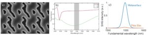
Second harmonic generation enhancement in freeform metasurfaces
In recent years, the use of metasurfaces has garnered extensive interest in the scientific community due to their potential application in a broad range of photonic applications. Devices based on metasurfaces enable new optical functionalities offered by their capability to manipulate light and re-emit it with on demand frequency, phase, radiation, and polarisation patterns. In dielectric metasurfaces, the efficiency of frequency conversion processes has been increased through the strong field enhancement generated at the resonant wavelengths [1]. Among the various nonlinear optical processes employed for frequency conversion, second-harmonic generation (SHG) is one of the most widely explored. SHG is a second-order nonlinear effect that coherently doubles the frequency of the incident light. However, to date, dielectric metasurfaces rely on conventional designs to enhance the conversion efficiency of SHG and even higher conversion efficiencies are required to meet the many applications associated with resonant frequency conversion in metasurfaces. Therefore, designs based on more complex topological features have been proposed [2,3].
Here, we demonstrate enhanced SHG using a GaAs metasurface designed by topology optimisation. We realise a resonant GaAs metasurface having a freeform design of increased geometric and fabrication complexity (Fig. 1a, b). The metasurface was fabricated by epitaxy, electron beam lithography and etching processes. Subsequently its linear transmission spectrum was measured showing a resonant behaviour around the telecommunication window, corresponding to a quality factor of ~ 40. The fabricated metasurface was illuminated by a fundamental beam having a central wavelength of 1550 nm, generating a strong SHG. Driven by the resonant behaviour, the metasurface shows an enhancement of up to 30 times in the SHG emission as compared to the GaAs thin film (Fig. 1c). Our results open new avenues for novel nonlinear imaging and sensor devices.

Passive and tunable dielectric metasurfaces
Novel flat optics based on nanoantennas and metasurfaces has recently emerged as a new approach to precisely control and manipulate light at nanoscale dimensions. Multiple functionalities, which are hard or impossible to achieve with conventional bulk optics, have been demonstrated with metasurfaces, which have additional advantages of smaller size, weight, and cost, when produced by large scale lithographic techniques. Additionally, when combined with tunable materials, metasurfaces can enable a variety of new applications including solid-state LiDARs for autonomous vehicles and fully 3D holographic displays. In this talk, I will first show our progress on developing passive/static metalenses, which can achieve various unique functionalities such as extremely high (~0.99 in air) numerical aperture or extra-large field of view (~180°). I will also show how by combining multiple lenses and controlling their dispersion we can enable white-light imaging in the visible spectrum and hyperspectral imaging in the mid-wave IR. Finally, I will focus on tunable metasurfaces, particularly demonstrating single pixel tunability in both 1D and 2D pixel arrays, providing the first demonstration of nanoantenna spatial light modulators with ~1 micron pixel size.

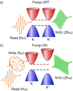
Ultrafast All-Optical Valleytronics in Transition Metal Dichalcogenide Monolayers
With conventional electronics reaching their performance limits in terms of speed and size, light is the ideal candidate to realize devices operating with high speed and low power consumption thanks to all-optical operations [1] and lightwave electronics. A promising approach in this direction is based on valleytronics using two-dimensional transition metal dichalcogenides (TMDs). TMD monolayers are direct gap semiconductors with two energetically degenerate but non-equivalent valleys in the K and K’ points of the Brillouin zone, owing to their honeycomb lattice structure. The valleys can be selectively excited (write) with one-photon CW excitation, nonlinear two-photon excitation, and coherent excitation by optical Stark and Bloch-Siegert shift because light of opposite helicity couples to opposite valleys. The detection (read) of valley polarization (VP) is so far mostly based on polarization-resolved photoluminescence (PL), since the (one-photon) spontaneous emission from the valleys follows the same selection rules as the (one-photon) excitation [2]. However, this approach has two main drawbacks: (1) it detects an averaged light emission over a time scale that is much longer compared to the valley and spin lifetimes; (2) it is intrinsically an invasive method, which measures the VP only after light emission. Nonlinear optics and in particular second harmonic generation (SHG) overcomes these disadvantages and provides an ultrafast and non-destructive method for the detection of the VP in TMDs [3]. The presence of a VP breaks the time-reversal symmetry of TMDs, reducing the intrinsic D3h crystal symmetry to C3h and thereby leading to new terms in the nonlinear optical susceptibility. These terms can be probed by polarization-resolved SHG measurements.
Fig. 1. Write and read mechanism of VP. a) Without a circularly polarized write pulse (pump-OFF) the polarization of the SH signal generated by the read pulse is determined solely by crystal symmetry. b) VP is generated by the optical Stark effect induced by a circularly polarized write pulse (pump-ON), resulting in a rotation of the emitted SHG with respect to the pump-OFF case.
In this work [4], we simultaneously pump (write) and probe (read) the VP in WSe₂ with one single elliptically polarized ultra-short pulse at room temperature. We probe the VP using polarization-dependent SHG measurements at different values of the fundamental wavelength corresponding to below-gap, 1s, and 2p exciton resonances and find that resonant SHG at the 1s state is the best probe of the VP. In addition, we investigate the mechanism of VP generation under our experimental conditions of below-gap excitation. Looking at the combined results of two-photon PL measurements and power-dependent valley SHG, we deduce that the VP observed in our experiments is generated by an ultrafast coherent optical Stark-shift (Fig. 1), which has been recently shown to be valley selective in TMDs [5]. Our work provides direct evidence of ultrafast and all-optical coherent generation and detection of valleys in atomically thin semiconductors.

Nanowire receivers enable polarimetry of THz metasurfaces
As next generation wireless communications approach the THz frequency band, there is a growing need for compact and scalable THz emitters, receivers, optical components and modulators. Unfortunately, traditional THz components are not just bulky but also expensive, making them unsuitable for mass market applications. However, recent advances in THz metasurfaces and nanowire-based THz devices offers us a path towards cheaper and far more compact THz components.
A strong optical and electrical polarization anisotropy makes nanowires ideal for applications in THz radiation detection and polarimetry. This anisotropy is associated with dielectric contrast with the environment, selection rules in novel crystalline polytypes, and quantum confinement.[1] Previously, we have used terahertz spectroscopy to study ultrafast charge-carrier dynamics in single-crystal III-V semiconductor nanowires. These studies revealed very high charge-carrier mobilities, the tunability of charge-carrier lifetimes, and picosecond switching times.[2] These results combined with the low capacitance of devices incorporating nanowires, identify them as ideal building blocks for THz frequency devices.[3]
We have utilised the polarization selectivity of individual nanowires to create a nanowire-based THz receiver [4] that records the full polarization state of THz pulses. An illustration of the hash nanowire device is shown in the Figure. Our hash nanowire devices are proving useful in the development and characterisation of THz metamaterials. Our detector has revealed the rotation of THz electric field from a twisted split-ring resonator, and novel THz metasurfaces developed through TMOS collaborations. These metasurface devices are compact and show promise as components for future THz communications systems.

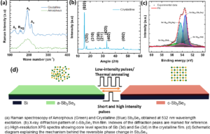
Multi-level switching in a low-loss phase change material, Sb2Se3
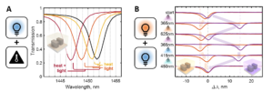
Phase change materials play a pivotal role in optics by introducing tunability, enabling dynamic control over optical properties. This tunability is essential for designing versatile photonic devices that can adapt to changing operational requirements, from optical switches to reconfigurable lenses. With their ability to switch between distinct structural states in response to external stimuli, phase change materials empower the development of agile and adaptive optical systems, driving innovation in telecommunications, photonics, and beyond. While explorations have primarily focused on certain PCMs, such as Ge2Sb2Te5 (GST) and Ge2Sb2Se4Te (GSST), recent studies highlight antimony-based chalcogenides like antimony trisulfide (Sb2S3) and antimony triselenide (Sb2Se3) as promising alternatives [1].
Sb2Se3 offers a broader operational spectrum with lower absorption losses in both its amorphous and crystalline phases, making it more versatile for various optical applications compared to Sb2S3. Additionally, its refractive index closely matches that of silicon, simplifying integration into photonics and enabling improved device performance. Moreover, the high optical contrast between amorphous and crystalline states, coupled with energy efficiency and rapid switching speeds, positions Sb2Se3 as a promising choice for advancing tunable and reconfigurable optical devices [2][3].
In this work, we systematically examine the deposition condition and optimization of near-stoichiometric Sb2Se3 films, investigating their structural and optical properties. We specifically explore the optical and electrical switching behavior exhibited by the film in both its amorphous and crystalline phases, aiming to provide a detailed understanding of these transitions. One noteworthy aspect of our research involves the demonstration of multilevel switching within the film. This breakthrough highlights the film’s capacity to exist in intermediate states, expanding its potential applications in advanced optical devices. Furthermore, our study delves into the practical utility of Sb2Se3 as a phase-change material by implementing an Sb2Se3-based phase-change memory. This memory device exhibits repeatable and reliable switching between its crystalline and amorphous states. Notably, we achieved a remarkably high switching ratio of approximately 104.
These findings contribute significantly to the broader understanding of Sb2Se3’s potential in the realm of integrated photonics.

[1] M. Delaney, I. Zeimpek is., D. Lawson, D. W. Hewak and O. L Muskens Advanced Functional Materials 30 (2020)
[2] W. Jia, R. Menon and B. Sensale-Rodriguez Optical Materials Express. 11, 9 (2021).
[3] M. Wang, J. S. Lee, S. Aggarwal, N. Farmakidis, J. Tan, H. Bhaskaran, (Conference on Lasers and Electro-Optics (CLEO),2022), pp 1-2.

Analog image processing with nonlinear nonlocal flat optics
Digital signal processing has revolutionized many fields of science and engineering, but it still shows critical limits, mainly related to the complexity, power consumption, and limited speed of analogue-to-digital converters. A long-sought solution to overcome these hurdles is optical analog computing. In this regard, flat optics has been recently unveiled as a powerful platform to perform data processing in real-time, with low power consumption and a small footprint [1, 2, 3]. So far, these explorations have been limited to linear optics. Arguably, significant more impact may be garnered from pushing this operation towards nonlinear processing of the incoming signals. In this context, we demonstrate here that nonlinear phenomena combined with engineered nonlocality in flat optics devices can be leveraged to synthesize Volterra kernels able to outperform linear optical analog image processing.

Multiple Stimuli-Responsive Polymer Coated Metasurfaces
Careful design of a 2D array of the sub-wavelength nanoresonators of a metasurface, known as meta-atoms, has enabled unprecedented control over light-matter interactions and led to the development of ultrathin optical devices including filters, lenses, displays and sensors[1]. For the vast majority of fabricated metasurfaces, the constituent meta-atoms are designed for a specific application and cannot be manipulated after fabrication. To broaden the application of optical metasurfaces to dynamic displays, optical switches, and arbitrary wavefront manipulators, the realization of efficient, tuneable metasurfaces is paramount. To date, most reports of tuneable metasurfaces employ a single electric, optical, mechanical, thermal or chemical stimulus to tune the optical resonance.
Polymer coatings provide a particularly attractive avenue for metasurface resonance tuning owing to the plethora of stimuli responsive organic molecules that can be incorporated onto a polymeric backbone [2]. In particular, combining multiple stimuli-responsive units into a single polymer enables heightened control over the resonance tuning, and can improve the functionality of the optical device.
Recently we reported coating silicon metasurfaces, hosting quasi-BIC resonances, with dual stimuli responsive polymers containing light-responsive azobenzene and temperature responsive triethylene glycol acrylate molecules [3]. The resulting device enabled dual stimulus tuning of the optical resonance (refer Fig. 1a). While either optical or thermal stimuli could be employed independently and induce modest resonance shifts, using the dual stimuli of light and temperature produced fully recoverable resonance shifts up to 5 nm and 62% transmission modulation.
We have further exploited the different absorption spectrum of spiropyran (SPA) and azobenzene (AZO) photoswitches, to enable two-colour, spatially resolved metasurface resonance tuning. When a silicon metasurface hosting quasi-BIC resonances is coated with polymers containing SPA or AZO; UV light induced a 15 nm redshift, and 4 nm blueshift in the metasurface resonance, respectively, as depicted in Fig. 1b. Enhanced functionality is achieved owing to the fact that the two photoswitches – and hence metasurface resonances – can be recovered with different visible wavelengths. The transmission values at the initial resonance wavelength and shifted resonance wavelengths, has potential application for logical processing and trainable models for diffractive optical neural networks.

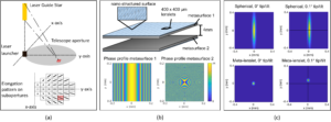
Anamorphic Meta-Lenslets for Laser Guide Star Wavefront Sensing
The Giant Magellan Telescope will use Laser Tomography Adaptive Optics to correct aberrations over a large fraction of the sky. It will be equipped with laser launchers, located around the periphery of the primary mirror, to excite artificial guide stars in the sodium layer of the atmosphere (altitude ∼95 km). However, the physical properties of the laser guide star present challenges for wavefront sensing with a Shack-Hartmann. A laser guide star is a vertically elongated shape due to the finite thickness of the sodium layer [1]. This results in each subaperture in a wavefront sensor imaging a unique perspective elongation radially dependent on its distance from the laser launcher, see Fig. 1(a). The maximum anamorphic ratio for a 40 m class telescope is ∼1:10. A standard solution is to use a large pixel scale to avoid excessive truncation of the elongated spots, but this approach greatly increases the readout noise and thereby limits sensitivity.
We suggest that flat nanostructured metasurfaces present a nuanced optical solution, where each meta-lenslet fabricated for an array can have a custom anamorphic ratio and elongation axis angle. Whereas Shack- Hartmann operation was previously demonstrated with arrays of single-layer dielectric metalenses [2], the parfocal operation across a broad range of magnifications requires a metasurface doublet configuration [3]. We identify original designs of multiple anamorphic meta-lenslet pairs for anamorphic ratios from 1:1 to 1:10, optimised for operation with the same distance from the detector plane. Depicted in Fig. 1(b) is the bilayer arrangement and the phase profiles for the two meta-lenslets for the largest required anamorphic ratio of 1:10. The Optics Studio (Zemax) simulation of our bilayer meta-lenslet showed that the spot size was reduced to a 1:1.7 ratio; resulting in a significantly smaller spot size than a conventional spherical lenslet, shown in Fig. 1(c) along with the measured displacements induced by a 0.1◦ tip-tilt field. The results of this study show a meta-lenslet array could achieve anamorphic compression with a compact optomechanical layout. Further developments of this study will include a prototype meta-lenslet array fabricated to validate the performance compared to the simulations. Figure caption: (a) Depiction of the radial dependency of spot elongation due to the finite thickness of the sodium layer in the atmosphere. (b) Bilayer arrangement of the meta-lenslet, with a 4 mm air gap. Phase profiles for the two metasurfaces for an anamorphic ratio of 1:10. (c) Normalised focal spot profiles for a spherical lenslet and the meta-lenslet, for an anamorphic ratio of 1:10. For an input tip-tilt wavefront of 0.1◦, the centroid is displaced 3×3 μm in x and y for the spherical, and is displaced 21×3 μm in x and y for the meta-lenslet.

Normal Incidence Nanowire Quantum Well Infrared Photodetectors
Since the first demonstration in 1987, III-V semiconductor-based quantum well infrared photodetectors (QWIPs) employing intersubband transition have facilitated mid- to long-wavelength infrared (IR) photodetection and thermal imaging with excellent pixel operability, uniformity, and stability. However, existing QWIPs are based on epitaxially grown planar structures containing in-plane quantum wells, in which intersubband transition at normal incidence is forbidden by light polarization selection rules. To overcome this limitation, additional processing steps are often required to fabricate optical gratings on the device surface, which, without careful design and optimization, could compromise the device performance.[1] The simplest way to break the selection rules is to build vertical quantum wells, which is unachievable with traditional planar growth processes. Semiconductor nanowires have been extensively studied over the past few decades with much insight gained on controlling the growth of nanowire heterostructures along not only axial but also radial directions on the nanowire sidewalls, providing excellent platforms for breaking the selection rules. In this work, we report, for the first time, a QWIP device based on nanowires embedded with five layers of radial InGaAs/InP quantum well (QW). Notably, normal incidence IR photodetection has been successfully demonstrated in the nanowire QWIP (NwQWIP), owing to the unique radial growth direction of the QW layers. Furthermore, at an operating temperature of 108 K, the NwQWIP features a sensitive photoresponse in the mid-wavelength IR band with a peak responsivity and detectivity of 120 mA/W and 1.3×10⁷ Jones at 4.2 μm, respectively. With a scalable and highly uniform fabrication process that boasts precise control over the growth direction of QW layers, the NwQWIP opens up great opportunities for next-generation large-scale, low-cost, and high-performance IR focal plane arrays.
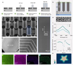
Nanowire quantum well infrared photodetector – growth, characterization, fabrication,
calibration, and imaging. A. Quantum well nanowires are grown by predefined the growing area on
the substrate via MOCVD.[2] B. 30° tilted view SEM image of InGaAs/InP nanowire array. C. STEM
of the longitudinal profile of the nanowire showing the lateral and axial growth of InGaAs quantum
well. D and E, STEM image of transverse profile of the nanowire showing clearly the 5 quantum wells
(~2-3 nm). F. EDX mapping of the cross-session in E. G. Device structure of NwQWIPs. H. A typical
SEM image shows the nanowires surrounded by SU8. I and J. Responsivity (I) and detectivity (J) of
the NwQWIPs at 108K. K. Infrared (3815 nm – 6000 nm) single-pixel imaging of a 1000℃ blackbody
light source.
References
[1] C. Jagadish et al., Advances in Infrared Photodetectors, 1st ed.; Academic Press Elsevier:
Cambridge, MA, USA , 2011; Volume 84.
[2] F. L. Zhang et al., Adv. Func. Mater. 2022, 32, 2103057.

Nanophotonics with a twist
Ultrathin meta-optics has transformed recent photonic design. I will highlight a new 3D meta-optics platform with unleashed height degree of freedom for both wavefront engineering and ultrahigh-sensitivity molecular sensing. In this talk, I will discuss the design, 3D laser nanoprinting, and applications of various 3D metasurfaces.
I will also introduce our recent development of nanophotonic chips for on-chip detection of twisted light modes. Selective control of light is essential for optical science and technology with numerous applications. I will review nanophotonic waveguides and integrated couplers used for selective coupling and spatial control of multiple degrees of freedom of light. I will highlight our recent development of hybrid nanophotonic circuits for optical logic operations and on-chip information processing. I will present the design and application of an OAM-controlled hybrid nanowire circuit for optical logic operations including AND and OR gates, as well as of an active hybrid nanophotonic circuit that enables nonlinear optical selectivity based on the spin and OAM of light.

Metamaterial mirrors for hybrid MEMS optical spectrometers
We report on the performance of hybrid micro-electromechanical systems (MEMS) optical spectrometer design in which one or both of mirrors of a Fabry-Perot structure is composed of a 2-dimensional metamaterial reflector [1] [2] [3]. Composed of a single layer of structured material, the suspended metamaterial mirror provides immense advantages over standard multi-layer mirror designs by allowing high reflectivity while minimizing stress-induced bowing. The single-layer suspended-mirror design also minimizes bowing that results from mismatched thermal expansion and, thus, allows for operation in cryogenically cooled hyperspectral imaging systems.
The metamaterial mirror design was developed using rigorous coupled wave (RCWA) analysis, and optimized for ultra-high reflectivity (greater than 99%) over a broad wavelength range. The design-work examined the sensitivity of the metamaterial mirror reflectivity to the mirror design parameters in order to optimize mirror reflectivity and spectral range. Metamaterial mirror reflectivity of over 99% were demonstrated over broad ranges (1800 nm – 2500 nm, 3720 nm – 5000 nm) in both the shortwave infrared (SWIR) and midwave infrared (MWIR) wavelength bands. However, it is observed that the incorporation of a metamaterial mirror with such high reflectivity reduces the free-spectral range of the Fabry-Perot filter, and this reduction is further exaggerated by the incorporation of a second metamaterial mirror.
The performance of the fabricated metamaterial mirrors provides good agreement with the RCWA modelling in both the SWIR and MWIR wavelength ranges. Fixed filter devices fabricated for the MWIR, wavelength range, containing a single metamaterial mirror, demonstrated high optical transmission (70%). The spectral full-width-half-maximum (FWHM) resolution of the measured filter device was 8 nm at room temperature, increasing to 10 nm when cooled to 80 K. While this FWHM width is broader than the model performance (4 nm), it is significantly narrower than previous reports.
![]()


Control of Spontaneous Emission with Semiconductor Metasurfaces: from Single Photons to Ultrafast Beam Steering
Metamaterials and their 2D implementation – metasurfaces – have been used extensively for wavefront manipulation since their inception nearly two decades ago. This has led to a revolution in optics due to the ability to design optical components with functionality and form factor that was unthinkable not long ago. Another use of metasurfaces relies on the ability to tailor distributions and intensities of local electromagnetic fields to study a variety of fundamental phenomena in light-matter interaction, 1 create novel tunable and active devices 2 and enhance optical nonlinearities.3-5 In particular, metasurfaces made from III-V semiconductors 6 offer an excellent platform for controlling spontaneous emission, as single and ensembles of quantum emitters can be embedded inside the meta-atoms. 7 In this talk I will focus on our recent work of ultrafast beam steering of spontaneous emission 8, and on recent results on single-photon emission from local-droplet epitaxy (LDE) single quantum-dots embedded in III-V metasurfaces. For the beam steering work, we demonstrated steering of incoherent spontaneous emission over 70 degrees and at subpicosecond timescales, using reconfigurable spatial momentum profiles created optically and projected on the metasurface sample. For single photon emission from LDE-QDs, we use Huygens metasurfaces to enhance collection efficiency by more than 20-fold, and show how this platform enables measurements of g(2) at excitation power densities that are much lower than what has been used previously.
- R. Sarma, N. Nookala, K. J. Reilly, S. Liu, D. de Ceglia, L. Carletti, M. D. Goldflam, S. Campione, K. Sapkota, H. Green, G. T. Wang, J. Klem, M. B. Sinclair, M. A. Belkin and I. Brener, Nano Lett 21 (1), 367-374 (2021).
- A. Benz, I. Montano, J. F. Klem and I. Brener, Applied Physics Letters 103 (26), 263116 (2013).
- R. Sarma, J. Xu, D. de Ceglia, L. Carletti, S. Campione, J. Klem, M. B. Sinclair, M. A. Belkin and I. Brener, Nano Letters 22 (3), 896-903 (2022).
- S. Liu, P. P. Vabishchevich, A. Vaskin, J. L. Reno, G. A. Keeler, M. B. Sinclair, I. Staude and I. Brener, Nature Communications, 1 – 6 (2018).
- T. Santiago-Cruz, S. D. Gennaro, O. Mitrofanov, S. Addamane, J. Reno, I. Brener and M. V. Chekhova, Science 377 (6609), 991-995 (2022).
- S. Liu, G. A. Keeler, J. L. Reno, M. B. Sinclair and I. Brener, Advanced Optical Materials 4 (10), 1457-1462 (2016).
- S. Liu, A. Vaskin, S. Addamane, B. Leung, M. C. Tsai, Y. Yang, P. P. Vabishchevich, G. A. Keeler, G. Wang, X. He, Y. Kim, N. F. Hartmann, H. Htoon, S. K. Doorn, M. Zilk, T. Pertsch, G. Balakrishnan, M. B. Sinclair, I. Staude and I. Brener, Nano Lett 18 (11), 6906-6914 (2018).
- P. P. Iyer, N. Karl, S. Addamane, S. D. Gennaro, M. B. Sinclair and I. Brener, Nature Photonics (2023).

Mode management and brightness enhancement in PT-symmetric, bottom-up micro-cavity lasers
In quantum mechanics, a non-Hermitian Hamiltonian can exhibit completely real eigenvalues if it obeys the parity-time (PT) symmetry [1]. In the past decade, the extension of the concept of PT symmetry into photonics has led to a plethora of research activities in developing a whole new class of photonics devices that operate based on PT-symmetric exceptional points (EPs), such as PT-symmetric lasers [2-4], EP-enhanced sensors [5], and coherent perfect absorbing (CPA) anti-lasers [6]. Among these novel devices, PT-symmetric lasers are especially attractive from the perspective of practical applications, as the optical coupling in the system can be engineered to achieve enhanced side mode suppression without compromising the lasing threshold and the fabrication complexity [2,3], which can potentially lead to high-power, single-mode lasing in miniaturised lasers. However, single-mode lasing in PT-symmetric micro-cavity lasers has so far only been demonstrated in systems fabricated by conventional top-down approaches. Meanwhile, bottom-up growth of III-V laser cavities has recently emerged as a promising alternative to the conventional top-down fabrication method, as it can potentially realise micro-cavity lasers with superior sidewall qualities, which is crucial to laser performance especially at the submicron dimensions. Despite the excellent fabrication qualities, similar to conventional micro-cavity lasers, bottom-up lasers also suffer from mode competition between a rich spectrum of transverse modes that are supported in the cavities. In this work, we realise PT-symmetric laser systems in bottom-up InP micro-ring laser cavities that are grown directly with a selective area epitaxy technique. By carefully optimising the optical coupling strength between the PT-symmetric cavity pair, we impose a PT symmetry breaking gain/loss threshold onto the system to achieve efficient side mode suppression and enhanced single-mode power output. Furthermore, with precise control over the growth rates of the sidewall facets of the laser cavities, we demonstrate tuning of the side mode suppression ratio by controlling the coupling gap between the PT-symmetric cavity pair. Notably, by engineering the sidewall facets of the bottom-up cavities, we also demonstrate enhanced optical coupling in cavity pairs with longer coupling lengths, which offers another degree of freedom in managing the lasing modes in the systems.

Advancing Nano- and Quantum Photonics with Machine Learning
Discovering unconventional optical designs via machine-learning promises to advance on-chip circuitry, imaging, sensing, energy, and quantum information technology. In this talk, we discuss photonic design approaches and emerging material platforms for showcasing machine-learning-assisted topology optimization for optical metasurface designs with applications in thermophotovoltaics, reflective optics, quantum photonic circuitry and lightsail technology. We demonstrate the effectiveness of autoencoders for compressing the vast design space of metasurfaces into a smaller search space. By employing global optimization via adjoint methods or quantum annealing, one can find the optimal metasurface designs within the smaller space constructed by the autoencoder. The techniques employed in this work extend well beyond the metasurface optimization space and into many inverse design problems for engineering and physics. We also apply machine learning approaches to advance quantum measurements and superresolution imaging.
Day 3 – Friday 15th December 2023


New Horizons for Nonlinear Space-Time Optics with Near-Zero-Index Materials
We explore materials where the real part of the permittivity (e)-epsilon is near zero (ENZ) and losses are small leading to a near-zero-index (NZI). ENZs and NZIs increase light-matter interactions via the enhanced fields at the interface between the ‘normal’ and ENZ materials, the “slow-light” effects and relaxed phase matching conditions. One important class of novel ENZ/NZI materials is transparent conducting oxides (TCOs) whose high-tunability have made them a leader in ENZ-enhanced nonlinear optics. Most recently, TCOs opened the door to exotic time-varying media phenomena such as negative refraction, time refraction, time reflection, photonic time crystals and other remarkable phenomena.

Meta-Optics are Bringing Uncooled IR Detection Near the Background Limit
The theoretical maximum performance of a broadband uncooled thermal detector is reached when the temperature fluctuations of the detector are dominated by radiation heat transfer and these fluctuations dominate all other noise sources. Commercial devices, such as the well known microbolometer camera are very far from this limit with noise typically dominated by electrical sources. However, recent metasurface research conducted by several groups around the world has allowed uncooled detectors to get tantalizingly close to the background limit and there appears to be reason for optimism that much but probably not all of the remaining gap can be closed.
One of the primary advantages of metal-dielectric metasurfaces is their ability to absorb large amounts of light using only a very thin set of films, often much less than a wavelength thick in total. Taking this concept a step further, one can try to design a metasurface that absorbs nearly 100% of incident light using a minimum amount of material, in other words, that has a high absorption per unit mass. Several research groups have made metasurfaces that have have high absorption per unit mass as an incidental part of their design. Our group at Minnesota, with an eye towards uncooled detection, has intentionally attempted to reduce the mass of high absorption structures and implemented designs that couple incident light into guided mode (intentionally broadband) resonances and utilize evanescent field coupling between pixels to ensure that even gaps participate in the absorption process.
Using these structures, we have recently demonstrated uncooled detectors operating at the thermodynamic fluctuation limit, where 98% of the noise is dominated by phonon and photon fluctuations. Phonon fluctuations are still larger than photon, but the devices are within about a factor of 3.6 of the background limit with room for improvement. The devices are read interferometrically from thermal expansion-induced deformations of the metasurface. The devices have an NETD of 4.5mK uncooled with a time constant of 7.4ms and a detectivity,
D* = 3.8 x 10^9 cm sqrt(Hz)/W, by far the highest ever achieved.
The talk will close with a perspective on future research possibilities and limits of thermal detectors: bolometric, thermoelectric, and optomechanical.
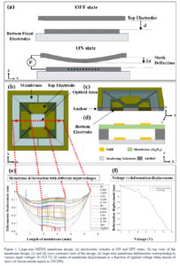
An Investigation of Large-area MEMS Structure for Tunable Optical Filter
Tunable Microelectromechanical systems (MEMS) optical filters using integrated micro-mirrors are well-known in infrared sensing technologies [1][2]. The transmission wavelength of a MEMS Fabry Perot spectrometer is controlled by electrostatically actuating the movable mirrors [2]. The electrostatic actuation force is generated by application of a voltage between two parallel conductive plates (electrodes), where one of the plates resides on the suspended movable structure. The electrostatic force causes the movable membrane to deflect downward towards the fixed bottom electrode, as shown in Figure 1(a).
For efficient light-coupling, as well as for imaging applications, large-area micro-mirrors are important [3]. However, the flatness specification of MEMS Fabry Perot mirrors is also critical important, which is greatly impacted by thin-film stresses [3]. Tensile stress and film thickness are commonly used parameters to maintain flatness of MEMS mirrors during actuation. However, thick and tensile membranes impose difficulties in actuation, resulting in high voltages being needed to achieve the wide range actuation. The objective of this research is to investigate and design a large-area and high-performance MEMS-based membrane structure with low voltage consumption.
Figure 1(b) depicts a 5.5 mm × 5.5 mm large-area membrane design with notches on all four corners to relieve biaxial strain. As the electrostatic force acting on the top electrode dramatically increases with the area of the electrode, two pairs of large electrodes (~1.8 mm × 2.5 mm) are placed on top of the silicon nitride membrane layer (300 nm thickness), as shown in Figure 1(d), with a separation gap d (approximately 2.2 μm) from the bottom electrode.
As shown in Figure 1(e) and (f), for a input low voltage (V=10.8 V DC), the maximum displacement of 0.38 μm can be achieved. According to Figure 1 (e), The centre optical area of the membrane, has a relatively flat surface with only ±30 nm height difference during actuation. Figure 1(f) shows that the displacement of the optical area is proportional to the square of applied voltage, which matches theoretical expectations. Future development necessary in this work is to overcome the balance issues in this large-area membrane that has resulted in tilting during actuation, along the x-axis, as shown in Figure 1(e).

Meta-optics for image processing and phase contrast imaging
With increasing concerns over energy consumption and processing speeds, there is an emerging interest in new all-optical approaches to manipulating images. Metasurfaces have been demonstrated to have significant potential for performing both image processing and optical analogue computing and provide a new avenue for extracting information from optical fields. They have been used in traditional 4f optical systems as novel spatial filters and can be designed to directly manipulate the spatial frequency content of an image. Although techniques such as edge enhancement have attracted widespread attention, visualisation of the phase of an optical field is another important application. This permits direct imaging of samples, such as unstained biological cells with weak absorption, without the requirement for staining. Traditionally phase imaging has been performed using methods including digital holographic and Differential Interference Contrast (DIC) microscopy that require relatively bulky, and sometimes expensive, components. Sophisticated computational strategies for extracting phase from intensity also exist, but these can be relatively slow. The use of metasurfaces provides an avenue to access this information directly, with reduced computational overhead, and using compact and potentially inexpensive devices. This presentation will discuss recent developments in nanophotonic approaches to all-optical image processing with a focus on phase imaging.

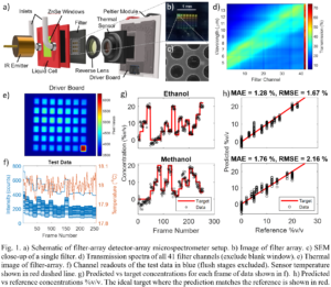
Simultaneous Determination of Methanol and Ethanol Concentration in Gasoline with Mid-Infrared Metasurface Filter-Array Microspectrometer
Mid-infrared spectroscopy (MIR; 2.5 µm to 25 µm) is typically only available in laboratories that have expensive benchtop Fourier-transform Infrared spectrometers. There is demand for low-cost, lightweight, and low-power consumption alternatives. An example application is identifying adulterated gasoline on-site. To reduce pollution from internal combustion vehicles, many countries are now recommending bioethanol as a fuel additive to reduce tailpipe emissions. There is concern however that this could lead to increased fuel adulteration, i.e. where retailers add excessive amounts of ethanol or even methanol (which is prohibited) to fool the consumer. Consumers could benefit by being able to check alcohol content in gasoline in-situ. A platform that could achieve this is the filter-array detector-array (FADA) microspectrometer (Fig. 1a). These combine thin, planar filters with a thermal detector to realise a simple and inexpensive microspectrometer that is robust against mechanical vibration. Yet to date, most demonstrations have only focused on binary detection of a single chemical relative to a non-absorbing background [Ref 1,2]. Here we demonstrate a FADA system that simultaneously tracks the concentration of ethanol and methanol in gasoline.
The experimental setup is shown in Fig. 1a. The liquid analyte is passed through a liquid cell (ZnSe windows) and is illuminated by an infrared source. The transmitted light then passes through a filter array (Fig. 1b) for spectral discrimination. The filter-array consists of a triangular lattice of micro-holes (Fig. 1c) in a thin aluminium layer (80 nm, on silicon substrate) that act as spectrally broad bandpass filters (Fig. 1d; tuned by varying lattice period). An array of 41 such filters (plus an additional blank window as reference) is imaged with a thermal camera (Fig. 1e). The intensity measured by the thermal camera for each filter can be thought of as the product of the source spectrum, analyte transmission spectrum, filter transmission spectrum, and camera responsivity spectrum, integrated over wavelength. The millimetre-sized filter-array is wholly imaged on a similarly sized thermal camera (microbolometer) by a reverse-lens setup. The thermal camera is mounted to a Peltier tile to stabilize the sensor’s temperature (18oC±0.1oC) to reduce unwanted intensity drift (Fig. 1f).
A total of 18 different gasoline/ethanol/methanol fuel blends are analysed, with thorough flushing of unadulterated gasoline between samples. The images are saved, filter channel readouts extracted, and a partial-least squares model (PLS-2) trained. To further compensate for intensity drift, the readouts during each flushing process are compared with the initial gasoline readouts and the subsequent sample measurements are re-scaled accordingly. The model is tested with fresh, unseen data (Fig. 1g) – the same 18 fuel blends are used again in a separate collection run. The mean-absolute error (MAE) and root-mean-square-error (RMSE) for ethanol is (1.28%, 1.67%) and for methanol is (1.76%, 2.16%). These results (Fig. 1h) are a first for detecting two different chemicals simultaneously in an absorbing background using a FADA microspectrometer. Further improvements can involve using a better thermal camera and spectral filters with narrower bandpass features.